Gerber File
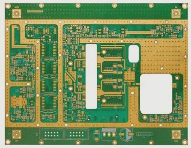
The Gerber file, exported from the PCB design, encompasses layers such as the Pad layer, solder mask layer, silk screen layer, and stencil layer. These files are essential for manufacturing. However, during the R&D phase, companies might be reluctant to disclose Gerber files due to concerns about plagiarism. In such cases, selectively providing only the necessary Gerber data for production while withholding sensitive information can be a prudent approach.
BOM
The Bill of Materials (BOM) provides a comprehensive breakdown of materials required for manufacturing. Each item in the BOM corresponds directly to components in the actual product, serving as a crucial reference for material procurement and production processes.
Coordinate File
The Coordinate File, which generates pick and place files, contains precise device location information. It should be formatted as .txt or Excel and must include the PCB origin, typically positioned in the lower-left corner.
Location Map
The Bit Number Map illustrates the placement of pads and silk screen layers, aiding in verifying correct SMT material positioning during assembly.