—
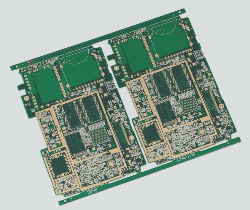
In the PCB board design process, wiring is a skill that is both limited and challenging. Even engineers with over a decade of experience often hesitate when faced with wiring tasks, fully aware of the various complexities and potential consequences involved. This uncertainty can sometimes hinder their confidence in executing optimal designs. However, there are true masters in this field. They possess a deep understanding of the technical aspects while infusing their work with a touch of creativity, resulting in wiring layouts that are not only functional but also visually appealing.
Below are some essential skills and considerations for effective wiring:
1. **Understanding PCB Layers**: PCB boards come in different layers—single-layer, double-layer, and multi-layer. Single-layer boards are less common nowadays. Double-layer boards are frequently used in audio systems, particularly in power amplifiers.
2. **Types of Via Holes**: Via holes play a crucial role in PCB design:
– **Through Holes**: These extend from the top layer to the bottom layer directly.
– **Blind Holes**: Extend from either the top or bottom layer to an internal layer but do not traverse through to the opposite side. This allows other layers to route around them without obstruction.
– **Buried Holes**: These vias are entirely contained within internal layers, invisible from the outer layers.
3. **Manual vs Automatic Routing**: Before engaging automatic routing tools, critical traces should be manually routed to meet specific requirements. It’s essential to ensure that input and output traces do not run parallel and adjacent to each other to prevent potential interference issues, such as reflections. Adding a ground wire for isolation when necessary can further mitigate these risks.
4. **Layout Considerations**:
– Lines on adjacent layers should ideally be routed perpendicular to each other to minimize parasitic coupling, which can occur when traces run parallel.
– Effective layout and adherence to routing rules—such as limiting the number of bends, vias, and trace lengths—significantly influence the success of automated routing processes.
5. **Optimizing Global Routing**: Initial routing typically involves quick connections of short lines, followed by more intricate labyrinth routing to optimize the overall signal path and ensure a robust wiring configuration.
In conclusion, mastering PCB wiring involves a blend of technical expertise and artistic intuition, resulting in functional and aesthetically pleasing designs.
—
This revision aims to clarify and enhance readability while maintaining the technical accuracy of the original content.

—
1. For layout, a fundamental principle is to separate digital and analog components as much as possible, ensuring that low-speed signals are not in proximity to high-speed signals. Another crucial principle is the separation of digital and analog ground planes. Digital grounding involves high-current switching operations, resulting in significant current flow during switching and minimal current flow when inactive. Therefore, digital and analog grounds must be kept separate to prevent interference.
2. Precautions for wiring between power supply and ground wires:
(1) Introduce a decoupling capacitor between the power supply and ground wires. The power supply should connect to chip pins via this capacitor. Decoupling capacitors serve two primary functions: providing instantaneous current to the chip and filtering power supply noise to minimize its impact on the chip and prevent noise generated by the chip from affecting the power supply.
(2) Widen power and ground traces as much as possible, ensuring ground traces are wider than power traces. The hierarchy is: ground traces > power traces > signal traces.
(3) Utilize large copper areas as ground planes. Unused areas on the PCB should be connected to ground, especially in multi-layer boards where each layer accommodates power, ground, and signal traces.
3. Handling of digital and analog circuit integration:
In modern PCBs, which often integrate digital and analog circuits, careful consideration is needed to mitigate mutual interference, particularly through ground noise. Due to the high frequency and sensitivity differences between digital and analog circuits, high-frequency signal lines should be positioned as far as possible from sensitive analog components. While the PCB’s overall ground plane should ideally have a single node, the integration of digital and analog circuit grounds must be managed within the PCB design, typically separating them except at specific interface points with external components.
4. Management of line corners:
Line thickness variations at corners can lead to reflections. Right angles are less ideal, while 45-degree angles are preferable and rounded corners can be beneficial depending on signal sensitivity. However, rounded corners complicate PCB design, so their use should be judicious, typically reserved for highly sensitive signal paths.
5. Verification of design rules post-wiring:
It is crucial to conduct thorough checks post-design to ensure compliance with production standards and operational requirements:
(1) Verify spacing between wires, components, and through-holes meets specifications.
(2) Confirm appropriate widths for power and ground traces, ensuring low impedance coupling.
(3) Implement special measures for critical signal lines, ensuring short lengths and separation of input and output lines.
(4) Ensure separate ground planes for analog and digital circuits.
(5) Check for potential signal short-circuits caused by graphics on the PCB.
(6) Make adjustments to unsatisfactory line shapes.
(7) Verify proper solder mask application and ensure no interference with electrical quality due to character logos on device pads.
(8) Avoid exposing power ground layer edges in multi-layer boards to prevent potential short circuits.
In conclusion, the aforementioned techniques and methodologies are based on experience and are invaluable for effective PCB design. Proficiency in design tools and software is essential, complemented by solid theoretical knowledge and practical experience. Attention to detail throughout the design process is critical to ensuring the final PCB meets quality standards and performs as intended.
—
This revision maintains the structure and content of the original text while improving clarity and readability through refined language and organization.


