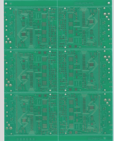
Latest Advances in PCB Processing Techniques
In the realm of printed circuit board (PCB) processing, the “pattern plating method” remains a common practice. This technique involves applying a layer of lead-tin anti-corrosion on the copper foil section designated to form the circuit pattern on the outer layer. Subsequently, the excess copper foil is chemically corroded through etching, resulting in the formation of two copper layers on the board. During the outer layer etching process, one copper layer is selectively removed, finalizing the circuit layout. Notably, the pattern plating method entails copper plating solely under the lead-tin resist layer.
Another notable approach is the “full board copper plating process,” where copper is uniformly plated across the entire board, except for areas shielded by photosensitive film. This method necessitates dual plating and etching across all board sections, which can pose challenges related to fine wire widths and side corrosion impacting line consistency.
For outer circuit processing of PCBs, a technique utilizing photosensitive film as the resist layer is commonly employed, mirroring inner layer etching procedures. Ammonia-based etchants, often paired with tin or lead-tin anti-corrosion layers, are widely utilized. Solutions such as ammonia/ammonium chloride or ammonia/ammonium sulfate are prevalent options.
Moreover, sulfate-based etching solutions enable copper separation for potential reuse via electrolysis owing to their minimal corrosion rate, albeit being less prevalent in production settings. While attempts have been made with sulfuric acid-hydrogen peroxide etchants, their commercial usage is limited due to cost implications and challenges in waste management, particularly concerning lead-tin resist etching.
Effective equipment calibration and handling of corrosive solutions are pivotal in ammonia etching processes. Sustaining uninterrupted operational status and selecting appropriate nozzle configurations and spray methods are imperative for achieving high-quality etching outcomes. The etching rate in ammonia etching is contingent on ammonia concentration, underscoring the necessity for fresh solutions to eliminate copper ions and facilitate the ammonia-triggered reactions.
Crucially, managing monovalent copper ions in ammonia etching solutions is crucial for enhancing reaction speeds, with additives employed to diminish monovalent copper ions. Introducing oxygen to convert monovalent copper to divalent copper aids in maintaining low monovalent copper levels, necessitating controlled airflow to prevent ammonia loss. Techniques like incorporating pure ammonia and employing pH meter control systems play a pivotal role in upholding solution stability.
Ongoing research in chemical etching has evolved towards machine structure design tailored for divalent copper solutions, presenting promising prospects for the PCB industry. Within the photochemical etching domain, stringent parameters are essential for etching thick copper foils, demanding elevated standards compared to traditional PCB practices.


