Types of PCB Etching
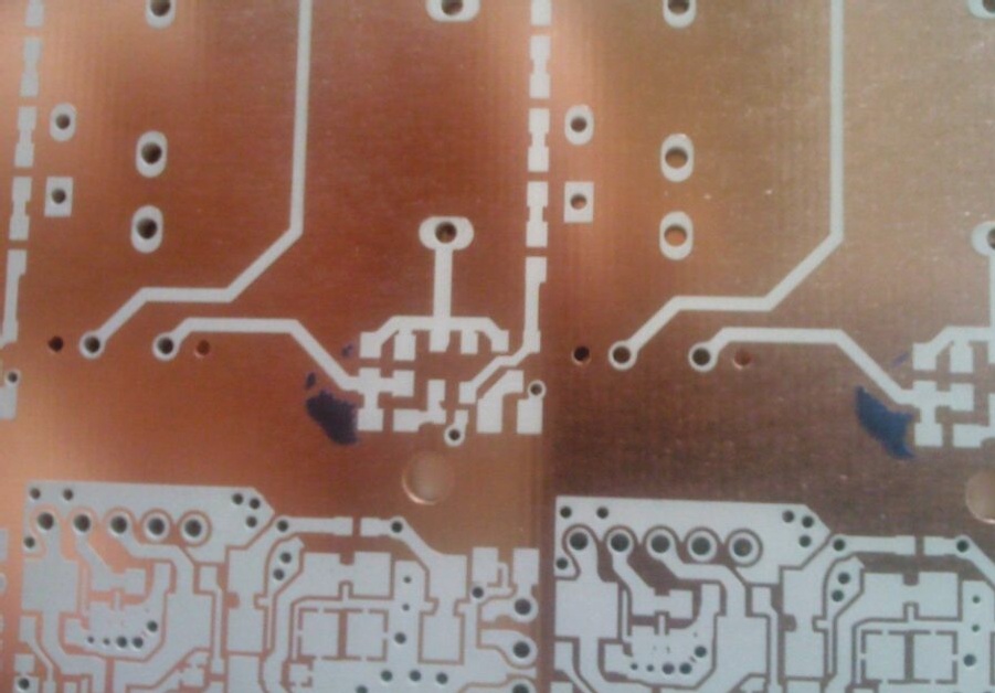
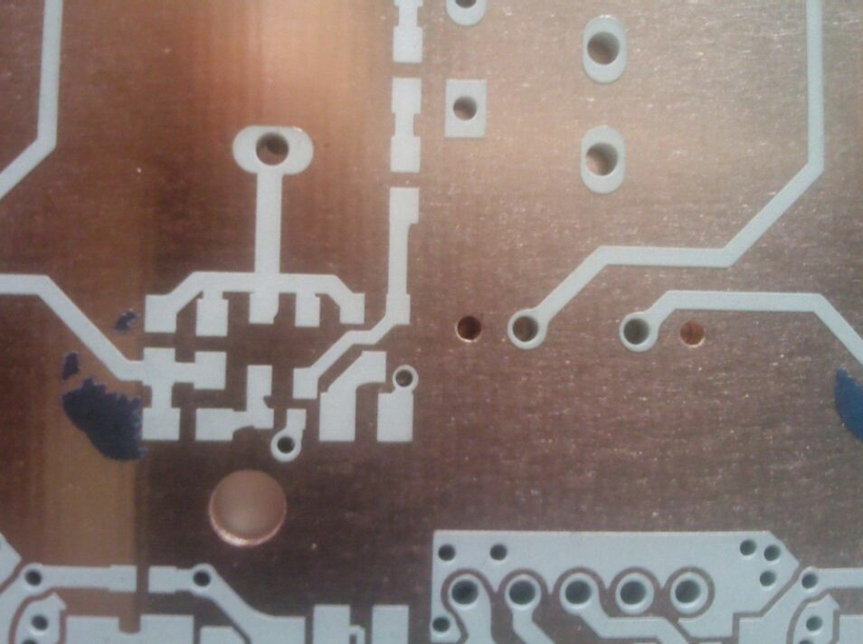
It’s important to note that during PCB etching, there are typically two layers of copper involved. In outer layer etching, only one layer of copper needs complete etching, while the rest forms the final circuit layout. This approach, known as pattern plating, features a copper plating layer exclusively beneath the lead-tin resist layer.
Alternatively, the “full board copper plating process” involves plating the entire PCB surface with copper, with only the photosensitive film areas protected by tin or lead-tin resist layers. However, this method requires double plating of copper across the entire board surface, leading to challenges during etching, especially with fine wire widths. Moreover, side corrosion can significantly impact line uniformity.
In outer circuit PCB processing, another technique employs photosensitive film instead of metal coatings as a corrosion-resistant layer. This method resembles the inner layer etching process used in PCB manufacturing.
Currently, tin or lead-tin resist layers are widely used in conjunction with ammonia-based etchants. Ammonia etchants, such as ammonia/ammonium chloride solutions, are preferred due to their non-reactivity with tin or lead-tin layers. Ammonia/ammonium sulfate etchants are also available commercially; however, their low corrosion rate limits their use in practical production scenarios, despite offering potential benefits in chlorine-free etching.
While sulfuric acid hydrogen peroxide has been explored for outer pattern etching, economic factors and waste liquid management have restricted its widespread commercial adoption. Additionally, this chemical combination is unsuitable for etching lead-tin resist layers and remains a secondary option in PCB outer layer production.

Printed Circuit Board (PCB) Etching Quality and Existing Problems
1. The basic requirement for etching quality is to completely remove all copper layers except under the resist layer. However, strictly defining etching quality must also consider the consistency of conductor linewidths and the extent of side corrosion. Due to the nature of current corrosive solutions, etching can occur not only vertically but also laterally, making side corrosion nearly unavoidable.
2. The issue of side etching is frequently debated in discussions of etching parameters. It is quantified as the ratio of side etching width to etching depth, termed the etching factor. In the PCB industry, this factor varies widely from 1:1 to 1:5. Ideally, minimal side etching or a low etching factor is preferred.
3. The design of etching equipment and the composition of the etching solution affect the etching factor and side etching extent. Some additives can mitigate side corrosion, though their exact chemical compositions are typically proprietary.
4. Etching quality issues often originate prior to the etching stage, during processes like film removal. The interconnectedness of various stages in PCB fabrication means issues in one area can propagate through subsequent stages, including etching.
5. During outer layer graphic etching, issues become more apparent due to the prominent “inverted stream” effect compared to other PCB processes. Etching, being the final step after a series of processes starting from film application and photosensitivity, magnifies issues accumulated from earlier stages.
6. Ideally, during graphic electroplating in PCB processing, the combined thickness of copper and tin or lead tin should not exceed the thickness of the photosensitive film. However, practical production often results in electroplated patterns thicker than the resist, leading to issues such as “edge” formation due to transverse accumulation of tin or lead tin.
7. Residual glue or film left under these edges prevents complete removal during film stripping, resulting in incomplete etching and the formation of “copper roots” that narrow line spacing, potentially leading to rejection by quality control standards.
8. In addition to chemical reactions, issues like residue accumulation in corrosive solutions can obstruct nozzles and pumps, necessitating shutdowns for maintenance that impact production efficiency.
9. Equipment adjustments and the interaction with corrosive solutions are crucial in maintaining consistent etching quality. Processes like ammonia etching are complex chemical reactions that require continuous operation once initiated to ensure consistent production.
10. Effective etching depends on maintaining the metal surface in constant contact with fresh etching solution, crucial for flushing out copper ions and providing necessary reactants like ammonia.
11. Control over monovalent copper ions in ammonia etchants significantly affects etching rates, with lower levels enhancing reaction efficiency. Techniques such as aeration help manage ion levels but must balance ammonia loss and pH stability.
12. Ongoing research in chemical etching, particularly in photochemical etching (PCH), explores alternative solutions like divalent copper, potentially offering stricter control parameters than traditional ammonia-based methods used in PCB fabrication.
These refinements and insights into PCB etching processes underscore the ongoing efforts to enhance quality and efficiency in printed circuit board manufacturing.
1. On the upper and lower plate surfaces, the etching states of the leading edge and the trailing edge differ significantly.
2. A large number of problems related to etching quality focus on the upper plate surface. It is crucial to understand this issue. These problems stem from colloidal structures produced by the etchant on the printed circuit board’s upper surface. Colloidal deposits on the copper surface affect both the jet force and block the replenishment of fresh etching solution, resulting in reduced etching speed. The formation and accumulation of colloidal structures cause varying etching degrees between the upper and lower graphics of the printed circuit board. Consequently, the initial part of the board in the etching machine may either be thoroughly etched or prone to over-corrosion due to the absence of accumulation and higher etching speed. Conversely, as subsequent parts enter the machine, accumulation has formed, thereby slowing down the etching speed.
3. Maintenance of Etching Equipment
4. The key factor in maintaining etching equipment is ensuring that the nozzles are clean and unobstructed. Blockages or deposits will affect the distribution of the etching solution under jet pressure. Unclean nozzles lead to uneven etching and can result in wastage of entire printed circuit boards.
5. Clearly, equipment maintenance involves replacing damaged and worn parts, including the nozzles. Nozzles are particularly prone to wear. Moreover, preventing excessive slagging buildup in the etcher is crucial, as it can disrupt the chemical balance of the etching solution. Excessive slagging can worsen chemical imbalance in the solution. The issue of slagging and buildup is critical; sudden large amounts of slagging in the etching solution typically signal a chemical imbalance. In such cases, thorough cleaning with strong hydrochloric acid or adjusting the solution composition is necessary.
6. Residual film can also contribute to slagging. Even a small amount of residual film dissolved in the etching solution can lead to copper salt precipitation and slag formation. This indicates incomplete removal of the previous film, often stemming from edge film and over-plating issues.


