What is a PCB board? When did printed circuit boards first come into use? Evolution of PCB PCB manufacturing process.
Finally, a process of copper plating on the borehole wall was developed. This allows electrical connections to be made between the circuits on either side of the board. Copper has replaced brass as the metal of choice because of its ability to carry electricity, its relatively low cost, and its ease of manufacture.
In 1956, the U.S. Patent Office issued a patent for a “process of assembling electrical circuits” sought by a small group of scientists represented by the U.S. Army. The patented process involves the use of melamine and other substrates and has been firmly laminated with a layer of copper foil. The wiring diagram was drawn and then photographed onto the zinc sheet. This plate is used to make plates for offset printing presses.
The acid-proof ink is printed on the copper foil of the circuit board and etched to remove the exposed copper, leaving behind the “printed wire”. Other methods have been proposed, such as the use of stencils, filters, handprints, and rubber stamping to deposit ink patterns. The holes are then punched with a die to match the location of the component leads or terminals. Insert the lead wire into the non-plating hole in the laminated material and then dip or float the card in the molten solder bath. The solder will cover the trace and connect the lead of the component to the trace.
They also used tinned holes, rivets, and washers to connect different types of components to the circuit board. Their patent even has a drawing showing two single panels stacked on top of each other, with a stand separating them. Each board has a number of elements at the top, one of which has a pin that extends through the top board to a hole in the bottom board, connecting them together, roughly trying to make the first multilayer board.
Much has changed since then. With the advent of electroplating technology, double-sided circuit boards were first allowed to appear on electroplating hole walls. Surface mount technology is the technology that we associate with the 1980s, and it was actually started in the 1960s twenty years ago. Gas masks were introduced as early as 1950 to help reduce corrosion that occurs on marks and components.
Epoxy compounds were spread across the surface of the assembly plates, similar to what we now know as conformal coatings. Eventually, the ink is silk-printed onto the panel before the printed circuit board is assembled. Block the area to be soldered on the screen. It helps keep the board clean and reduces corrosion and oxidation, but the tin/lead coating used to coat the trace can melt during welding, causing the mask to peel off. Because of the large spacing between the tracks, it was seen as a cosmetic issue rather than a functional one.
By the 1970s, as circuits and spacing became smaller, tin/lead coatings were still used to coat traces on board, and the traces began to be fused together during the welding process. The hot air welding method, which began in the late 70s, allows tin/lead stripping to eliminate problems after etching. A solder resists layer can then be applied to the exposed copper circuit, leaving only the plating holes and pads to avoid being covered with solder.
Trajectory work becomes more intensive as the hole continues to get smaller, flux bleeding, and registration issues on the dry film mask. They were mainly used in the United States, while the first photo-able masks were developed in Europe and Japan. In Europe, solvent-based “Probimer” inks are applied by curtain coating the entire panel. The Japanese centered on the silk-screen process using various water-based LPIs. All three mask types use standard UV exposure units and photo tools to define the pattern on the panel.
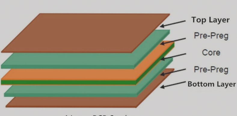
By the mid-1990s, water-based liquid light-able imaging masks dominated the industry with specialized equipment designed specifically for their applications. The complexity and increasing density that drives the development of solder resistance layers also force the development of copper tracks laminated between dielectric layers. Multilayer PCB was first used in the United States in 1961.
The development of transistors and the miniaturization of other components have led more and more manufacturers to use printed circuit boards in an increasing number of consumer products. Aerospace equipment, flight instruments, computer, and telecommunications products, as well as defense systems and weapons, are beginning to take advantage of the space-saving advantages offered by multilayer circuit boards. Surface mount devices are being designed to be compared to the size and weight of equivalent through-hole components. Then came the invention of the integrated circuit, and the boards continued to shrink in almost every way.
Rigid circuit boards and cable applications have given way to flexible circuit boards or combinations of rigid and flexible PCBs. These and other advances will keep the printed circuit board industry dynamic for years to come.


