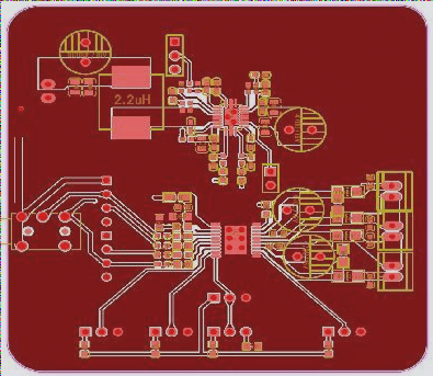
1. **Multilayer Circuit Board Wiring**
High-frequency circuits often feature high integration and dense wiring. Using multi-layer boards is not only necessary for effective wiring but also serves as a crucial method to reduce interference. During the PCB layout stage, selecting an appropriate board size with a suitable number of layers allows for optimal use of intermediate layers to create shields, implement nearest grounding, and effectively reduce parasitic inductance and signal transmission length. All these measures contribute to the reliability of high-frequency circuits, such as mitigating amplitude reduction due to signal cross-interference. Data indicates that, using the same material, a four-layer board can have noise levels 20dB lower than a double-sided board. However, a drawback exists: increasing the number of layers complicates the manufacturing process and raises the unit cost. Therefore, it is essential to choose the appropriate number of layers for the circuit board during PCB layout, plan component placement carefully, and adhere to proper wiring rules to ensure effective PCB design.
2. **Minimize Lead Bends in High-Speed Electronic Devices**
For high-frequency circuit wiring, it is best to use straight leads. If turning is necessary, it should be achieved using a 45-degree corner or a circular arc. This requirement enhances the mechanical strength of copper foil in low-frequency circuits. However, in high-frequency circuits, it also helps in reducing external emissions and mutual coupling of high-frequency signals.
3. **Minimize Lead Length Between Pins in High-Frequency Circuit Devices**
The radiation intensity of a signal is proportional to the trace length of the signal line. Longer leads for high-frequency signals are more prone to coupling with nearby components. Therefore, signals such as clock, crystal oscillator, DDR data, LVDS lines, USB lines, HDMI lines, and other high-frequency signal lines should be kept as short as possible.
4. The fewer lead layers that alternate between the pins of high-frequency circuit devices, the better. The principle here is that reducing the number of vias (Via) used in component connections improves performance. Each via can introduce approximately 0.5pF of distributed capacitance, so minimizing vias can significantly boost speed and reduce data errors.
5. Pay attention to the “crosstalk” introduced by parallel signal lines that are closely spaced. High-frequency circuit design must consider the crosstalk arising from parallel routing of signal lines. Crosstalk refers to unwanted coupling between signal lines that are not directly connected. High-frequency signals, transmitted as electromagnetic waves, can cause lines to act like antennas, emitting electromagnetic field energy and creating noise from mutual coupling. Factors such as PCB layer parameters, signal line spacing, electrical characteristics of both ends, and termination methods impact crosstalk. To minimize crosstalk, follow these guidelines:
– Insert a ground wire or ground plane between closely spaced signal lines to provide isolation and reduce crosstalk.
– If avoiding parallel routing is impossible, place a large ground area opposite the parallel signal lines to significantly reduce interference.
– Increase spacing between adjacent signal lines, minimize parallel length, and orient the clock line perpendicular to key signal lines if space allows.
– When parallel wiring on the same layer is unavoidable, ensure that the directions of adjacent layers’ wiring are perpendicular.
– In digital circuits, where clock signals with fast edge changes are prone to high crosstalk, surround the clock line with ground lines and add multiple ground holes to lower distributed capacitance and crosstalk.
– For high-frequency signal clocks, use low-voltage differential signals with ground wrapping and ensure proper integrity of the package ground punching.
– Unused input terminals should not be left floating; they should be grounded or connected to the power supply, as floating lines can act like antennas and cause interference. Grounding can inhibit emissions, and this method often shows immediate results.
6. Add high-frequency decoupling capacitors to the power supply pins of each integrated circuit block. Adding these capacitors near the power supply pin effectively suppresses high-frequency harmonics’ interference.
7. Isolate the ground wires of high-frequency digital signals from analog signal ground wires. When connecting analog and digital ground wires to a common ground, use high-frequency choke magnetic beads or direct isolation with single-point interconnection at a suitable location. High-frequency digital signal grounds often have inconsistent potentials and significant harmonic components. Direct connection can cause interference through ground coupling, so isolation or choke beads are preferred for maintaining signal integrity.