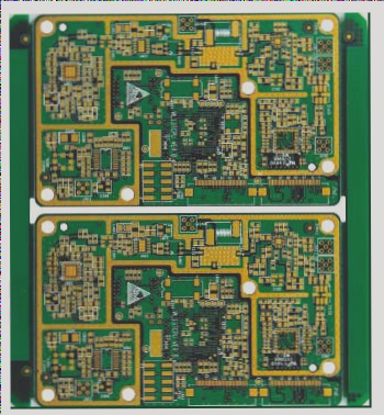
Printed Board Design Essentials
-
Correctness
Ensuring the accuracy of the electrical schematic is crucial in PCB design to avoid “short circuits” and “open circuits.” Advanced CAD software can help verify connections.
-
Reliability
While a circuit board may be correctly connected, issues like improper material selection and poor installation can lead to failure. Simpler structures and fewer components enhance reliability.

-
Reasonableness
The overall design of a PCB impacts its manufacturing, assembly, and maintenance. Design errors can increase costs and working hours, emphasizing the need for continuous improvement.
-
Economy
Striking a balance between cost-saving measures and quality is essential in PCB design. Opting for cheaper materials may lead to long-term issues, emphasizing the complexity of achieving true economic efficiency.
Expert Advice:
-
Establish Clear Design Direction
Consider factors like signal types and voltages to prevent interference. Linear signal paths are ideal, and proper isolation techniques can help overcome layout challenges.
-
Select Proper Grounding Point
A solid grounding point is crucial for PCB design. While achieving a common ground can be challenging, efforts should be made to consolidate ground lines for optimal performance.
Proper Power Supply Filter and Decoupling Capacitor Placement
One crucial aspect of PCB design is the proper placement of power supply filters and decoupling capacitors. Simply indicating the number of capacitors on the schematic is not enough; their exact placement is key. These capacitors are essential for filtering or decoupling switching devices like gate circuits. For optimal performance, they should be placed in close proximity to the components they support. Placing them too far away can diminish their effectiveness. Interestingly, when these capacitors are positioned correctly, issues with grounding points often diminish.
Quality Routing Matters
When it comes to routing on a PCB, attention to detail is crucial. Wide traces should be utilized whenever possible, and high-voltage or high-frequency traces should be routed with smooth, rounded corners to avoid sharp angles. Ground traces should be wide, and incorporating large copper areas significantly enhances ground connections’ effectiveness.
Post-Production Concerns and PCB Design
Many post-production issues can be traced back to the PCB design phase. Problems such as excessive via usage, careless copper sinking, and soldering difficulties often originate from design flaws. Minimizing via usage is important, as too many vias can introduce hidden risks. Careful consideration should also be given to the density of parallel traces in the same direction to prevent unintended connections during soldering. Proper spacing between solder joints is essential for manual soldering without compromising quality or efficiency. The size matching of pads or vias with hole sizes is critical—small pads can complicate manual drilling, while improper matching can lead to CNC drilling issues. Inadequately sized pads may result in drilling problems like “C” shaped holes or completely drilled-off pads. Thin traces and large unconnected copper areas are susceptible to uneven corrosion, leading to over-etching of thin traces or complete failure. Therefore, a well-thought-out copper coating design not only enhances grounding and reduces interference but also ensures the long-term reliability of the PCB.


