
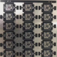
Printed Circuit Boards (PCBs) in Electronic Devices
- PCBs are essential components found in almost every electronic device, serving as the foundation for mounting electronic components.
- PCBs play a crucial role in establishing electrical connections between components, enabling the device to function properly.
- With the increasing complexity of electronic devices, PCBs are designed to accommodate a higher number of components, leading to denser circuits.
- Standard PCBs consist of a substrate made from insulating and thermally resistant materials, with copper foil circuitry creating conductor patterns for circuit connections.
Key Details About PCBs
- In single-sided PCBs, components are soldered on one side, while traces are on the opposite side, requiring holes for pin connections.
- Usage of sockets on PCBs allows for easy removal and reinstallation of components post-production.
- Edge connectors, like “golden fingers,” are used to connect multiple PCBs, such as interface cards to motherboards.
- The green or brown color on a PCB indicates the solder mask, protecting copper traces and aiding in correct component soldering.
- Single-sided boards have limitations on circuit layout, while double-sided boards offer more wiring area and are suitable for complex circuits.
Enhancing Electronic Connections
- Vias, small holes filled with metal, are crucial in double-sided PCBs to establish connections between traces on both sides.
- The silkscreen layer on PCBs provides component positioning information, aiding in assembly and maintenance.
- Understanding the different types of PCBs and their features is essential for designing efficient and reliable electronic devices.
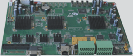
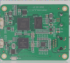
Multi-Layer PCBs: Enhancing Wiring Capacity
- Multi-layer boards utilize multiple wiring layers separated by insulating material.
- Number of layers varies, with most motherboards having 4 to 8 layers, but can reach up to 100 layers.
- Supercomputers often use multi-layered boards, but standard computer clusters are reducing the need for ultra-multilayered boards.
- Internal layers are tightly integrated, making it challenging to determine the total number without close inspection.
Vias in Multi-Layer Boards
- Vias in multi-layer boards can be optimized with technologies like buried vias and blind vias.
- Blind vias connect internal layers to the surface without traversing the entire board.
- Buried vias link internal layers and are invisible from the surface.
Layer Classification in Multi-Layer PCBs
- Each layer in multi-layer PCBs is directly linked to ground and power.
- Layers are categorized as signal, power, or ground layers.
- PCBs with components requiring different power supplies typically have more than two power and trace layers.
 العربية
 简体中文
简体中文 Nederlands
 English
 Français
 Deutsch
 Italiano
 日本語
日本語 한국어
한국어 Português
 Русский
 Español
 ไทย
ไทย