PCB Circuit Board Design Process Overview
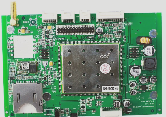
Before delving into PCB circuit board design, it’s crucial to grasp the concept of a Printed Circuit Board (PCB). A PCB consists of conductive patterns created from printed circuits, printed components, or a combination of both, arranged on insulating materials according to a specific design. These are commonly known as printed circuits.
History and Importance of PCB Technology
The PCB technology originated in 1936 and gained widespread usage in military radios in the United States by 1943. Since the mid-1950s, PCB technology has been extensively adopted across various industries. Today, PCBs are considered the foundation of electronic products, with applications spanning sectors like computers, telecommunications, consumer electronics, industrial automation, medical devices, defense, military, aerospace, and more.
Latest Updates in PCB Design
Recent advancements in PCB design have focused on enhancing component libraries and schematic diagrams. Engineers now prioritize establishing PCB component package libraries based on standard component size data before creating schematic (SCH) component libraries. This meticulous preparation ensures optimal PCB installation and correct pin mapping.
Key Steps in PCB Design
- Preliminary Preparation: Create component libraries and schematic diagrams.
- PCB Component Package Library: Engineer the library based on component size data.
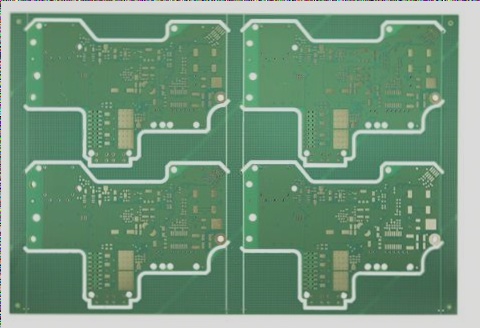
- PCB Structure Design: Draw the PCB frame and position components accordingly.
- PCB Layout Design: Place components within the PCB frame as per design specifications.
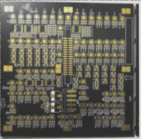
- PCB Routing Design: Implement routing in stages to optimize board performance.
- Routing Optimization and Silk Screen Placement: Continuously strive for design improvement and balance hardware requirements.
Expert Tips for PCB Design
Remember, PCB design is an art of compromise, aiming for continual improvement rather than perfection. Balancing various hardware requirements is key, and meticulous attention to detail during design stages ensures optimal performance and functionality.
PCB Design Optimization and Quality Control
When evaluating a PCB design, a circuit designer may need to make compromises due to cost constraints. For instance, opting for a 4-layer board instead of a planned 6-layer board can lead to signal quality issues like increased crosstalk between layers.
Routing Optimization and Post-Processing
It’s a common rule of thumb that optimizing routing takes twice the time of initial routing. After completing PCB layout optimization, post-processing steps are crucial. This includes placing silk screen labels on the PCB surface, ensuring that the bottom layer’s text is mirrored to prevent confusion with the top layer.
Netlist DRC Check and Structural Inspection
Quality control is vital in PCB design. Methods like design self-checks, peer reviews, and expert inspections help ensure design integrity. Netlist DRC checks and structural inspections verify that the PCB design aligns with schematic and structural requirements. Designers often follow personalized quality checklists, incorporating industry standards and personal experience.
PCB System Board Preparation
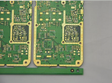
Prior to production, collaboration with the PCB supplier’s process engineer is essential. Discussions cover material selection, trace widths, impedance control, stack-up thickness, surface treatments, hole tolerances, and delivery specifications to address manufacturing queries effectively.
- If you require PCB manufacturing services, feel free to contact me.