
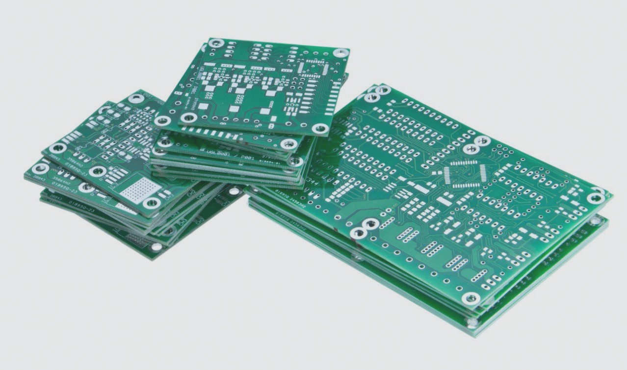
PCB Board Design Techniques for High Device Density
As the demand for smaller PCB board sizes and higher device density increases, PCB board design becomes more challenging. To achieve efficient routing and shorten design time, it’s essential to focus on PCB board planning, layout, and wiring techniques.
Determining PCB Board Layers
- Early in the design process, determine the board size and required routing layers.
- The number of wiring layers and stacking method directly impact trace routing and impedance.
- Design with more circuit layers and evenly distributed copper for better results.
Design Rules and Limitations
- Routing tools must adhere to correct rules and constraints for successful routing.
- Parameters like trace width, via count, and layer limitations significantly impact routing tool performance.
- Consider design requirements thoughtfully for successful routing.
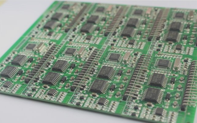
Layout of Components
- Design for Manufacturability (DFM) rules constrain component placement during assembly.
- Optimize circuit layout for automated routing while considering assembly constraints.
- Routing tools execute routing based on defined rules and constraints set by the designer.
Fan-Out Design
- Each pin of surface mount devices should connect to at least one via during fan-out design.
- Optimize automatic routing tool efficiency by maximizing via and trace sizes.
- Consider power and grounding influences on fan-out design.
Manual Wiring and Critical Signal Processing
- Manual routing complements automated tools in PCB design.
- Route critical signals manually or with automated assistance, followed by post-wiring inspection.
- Avoid arbitrary grounding connections to prevent circuit disruption, especially at higher frequencies.
Auto-Routing and Wiring Arrangement
- Control electrical parameters during auto-routing for critical signals.
- Configure auto-routing tools to align with design expectations and manage signal layers effectively.
- Manually evaluate and edit signal paths on the PCB for long-length signals with minimal constraints.


 العربية
 简体中文
简体中文 Nederlands
 English
 Français
 Deutsch
 Italiano
 日本語
日本語 한국어
한국어 Português
 Русский
 Español
 ไทย
ไทย