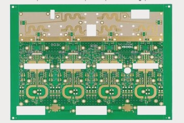
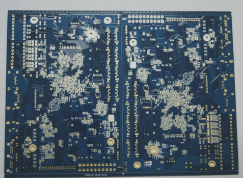
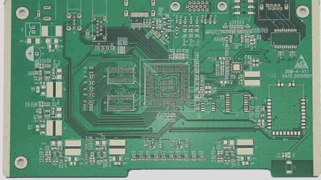
Experts summarize the characteristics, advantages, and disadvantages of various surface processes produced by PCB surface treatment technology. The solderability of bare copper itself is excellent, but it is prone to oxidation. To ensure optimal solderability and electrical properties of PCB products, technical experts have compiled the characteristics, advantages, and disadvantages of various surface processes.
**OSP**
Main feature: An organic protective film is applied to the copper surface.
Thickness control: 0.2–0.6 µm.
Advantages: Uniform film thickness and low cost.
Disadvantages: Struggles to withstand multiple reflow soldering cycles.
**Shen Yin**
Main feature: A silver layer is deposited on the copper surface via a displacement reaction.
Thickness control: 0.2–0.4 µm.
Advantages: Uniform silver layer, moderate cost, and extended storage period.
Disadvantages: Susceptible to oxidation, and discoloration or yellowing of the silver surface can hinder solderability.

**Shen Xi**
**Main feature:** A layer of tin is deposited on the copper surface through a displacement reaction.
**Thickness control:** ≥1.0 µm
**Advantages:** Uniform tin layer, average cost, easy aging process.
**Disadvantages:** The solution is prone to aging, and addressing tin whisker issues can be challenging.
**Spray tin**
**Main features:** A protective layer is obtained through physical means, specifically hot air leveling.
**Thickness control:** 2~40 µm
**Advantages:** Excellent solderability, high compatibility, and long storage life.
**Disadvantages:** Contains lead and has poor flatness.
**Lead-free spray tin**
**Main features:** Similar to spray tin, utilizing hot air leveling to create a protective layer.
**Thickness control:** 2~40 µm
**Advantages:** Simple process, serves as a substitute for tin spraying, and offers long storage life.
**Disadvantages:** Poor flatness, limited fluidity, and reduced solderability.
**Immersion Nickel Gold**
**Main feature:** A thin layer of nickel and gold is applied to the copper surface via a displacement reaction.
**Thickness control:** 0.05~0.1 µm
**Advantages:** Uniform coating, good solderability, and extended storage life.
**Disadvantages:** High cost and susceptibility to black disk issues.
**Nickel Palladium**
**Main feature:** A thin layer of palladium is deposited prior to gold immersion.
**Thickness control:** 0.05~0.1 µm
**Advantages:** Ideal for wire bonding and reduces gold costs.
**Disadvantages:** Not widely adopted in the industry.
**Electric hard gold**
**Main feature:** A thin nickel-gold layer is deposited on the copper surface through an electrochemical oxidation-reduction reaction.
**Thickness control:** 0.38~2.0 µm
**Advantages:** Offers wear resistance, oxidation resistance, and low electrical resistance.
**Disadvantages:** Poor solderability, high cost, and usage depends on performance requirements.
**Golden finger**
**Main feature:** A thin nickel-gold layer is applied on the copper surface through an electrochemical oxidation-reduction reaction.
**Thickness control:** 0.25~1.5 µm
**Advantages:** Excellent wear resistance, oxidation resistance, and low electrical resistance.
**Disadvantages:** Poor solderability, high cost, and usage depends on performance requirements.
**Full board gold-plated**
**Main feature:** A thin nickel-gold layer is deposited on the copper surface through an electrochemical oxidation-reduction reaction.
**Thickness control:** 0.025~0.1 µm
**Advantages:** Uniform coating, suitable for wire bonding.
**Disadvantages:** High cost.
The above is a summary of the surface treatment technologies for PCB circuit boards.


