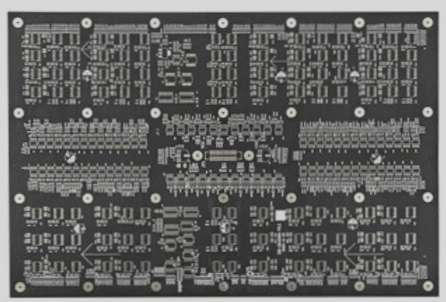
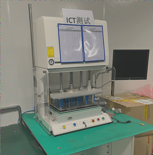
1. The PCB, or printed circuit board, serves as a critical provider of electrical connections for electronic components. Its development spans over a century, with the design primarily focusing on layout considerations.
2. The key advantage of using circuit boards is their ability to significantly minimize wiring and assembly errors, thereby enhancing automation levels and increasing production efficiency.
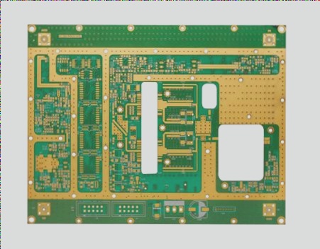
3. The basic composition of a circuit board includes pads, vias, mounting holes, wires, components, connectors, fill, and electrical boundaries. Each component has distinct functions as outlined below:
4. **PCB pads:** These are metal holes designed for soldering component pins.
5. **Vias:** Comprised of both metal and non-metal types, metal vias are utilized to connect component pins across different layers.
6. **Mounting holes:** These are employed to secure the circuit board in place.
7. **Wires:** Copper traces form the electrical network that links the pins of various components.
8. **Connectors:** These facilitate the interconnection of components across circuit boards.
9. **Filling:** This refers to the copper coating applied to the ground wire network, effectively reducing impedance.
10. **Electrical boundary:** This defines the dimensions of the circuit board, ensuring that all components remain within the specified limits.
11. **PCB substrate:** The substrate is generally classified based on its insulating properties. Common materials include bakelite, fiberglass, and various plastic types.
12. Typically, PCB manufacturers utilize an insulating layer made from glass fiber, non-woven materials, and resin, which is then combined with epoxy resin and copper foil to create a “adhesive sheet” (prepreg) for production.
13. The common base materials and their primary components are:
—
Let me know if you need any further adjustments!
1. **FR-1**──Phenolic cotton paper, commonly referred to as bakelite (more economical than FR-2).
2. **FR-2**──Phenolic cotton paper.
3. **FR-3**──Cotton paper, epoxy resin.
4. **FR-4**──Woven glass, epoxy resin.
5. **FR-5**──Glass cloth, epoxy resin.
6. **FR-6**──Masked glass, polyester.
7. **G-10**──Glass cloth, epoxy resin.
8. **CEM-1**──Tissue paper, epoxy resin (flame retardant).
9. **CEM-2**──Tissue paper, epoxy resin (non-flame retardant).
10. **CEM-3**──Glass cloth, epoxy resin.
11. **CEM-4**──Glass cloth, epoxy resin.
12. **CEM-5**──Glass cloth, polyester.
13. **AIN**──Aluminum Nitride.
14. **SIC**──Silicon Carbide.
**Basic Circuit Board Production**
Basic production processes can be categorized into two primary types based on technology: subtractive and additive.
**Subtractive Method**
The subtractive method involves using chemicals or machinery to eliminate unnecessary areas on a blank circuit board (i.e., a board coated with a full sheet of metal foil), leaving the necessary space for the required circuit.
**Screen Printing:** The pre-designed circuit diagram is transformed into a screen mask, with unnecessary circuit areas covered by wax or impermeable materials. The mask is then placed on the blank circuit board, and a protective agent is applied. The board is immersed in a corrosive liquid, eroding the uncovered areas, followed by cleaning the protective agent.
**Photosensitive Plate:** A transparent film mask of the pre-designed circuit is created (commonly using printer transparencies), with necessary parts printed in opaque color. A photosensitive paint is applied to the board, the mask is placed on it, and exposed to strong light for several minutes. After removing the mask, a developer reveals the pattern on the board, followed by the same etching process as in screen printing.
**Engraving:** A milling machine or laser engraver is employed to directly remove unnecessary sections on the blank circuit.
**Additive Method**
The additive method involves initially covering a substrate with a thin layer of copper, applying photoresist (D/F), exposing it to ultraviolet light, and developing it to reveal necessary areas. Electroplating then increases the copper thickness to the required specifications. A layer of anti-etching resist—thin metal tin—is plated, followed by the removal of photoresist (termed film removal), and etching away the copper foil beneath it.
**Industry Status**
As the production of printed circuit boards occurs in the latter stages of electronic equipment manufacturing, it is considered a downstream sector of the electronics industry. Nearly all electronic devices rely on printed circuit boards, making them the leading product in terms of market share within global electronic components. Currently, Japan, China, Taiwan, Western Europe, and the United States are the primary manufacturing hubs for printed circuit boards.

