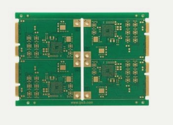
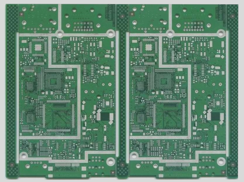
Green Paint Construction and BGA Installation Tips
Green Paint Construction
When soldering the ball pad at the bottom of the BGA of FR4 PCB, the “green paint limit” method is used. If the green paint layer is too thick (>1mil) and the pad surface is small, it can lead to a “crater effect” hindering wave soldering penetration. During ball planting, excess flux and heat can cause solder to seep under the green paint, leading to peeling. This differs from the solder paste method used in PCB processing pads.
Typically, if the SMD copper pad is slightly larger, the green paint can extend up to 4mil. However, tin flow limitations weaken the solder joint compared to NSMD joints, affecting joint strength and stress dissipation. This lack of dissipation can reduce the joint’s fatigue life to 70% of NSMD joints.
Designers and manufacturers often overlook these factors, compromising BGA bearing pad strength in mobile phone circuit boards during lead-free soldering.
- Green paint hole plugging: Facilitates vacuum pumping, board fixation during testing, and protection from tin surges during wave soldering.
- Re-wave soldering after reflow soldering: Use heat shields to prevent reflow-soldered ball pads from melting during additional component soldering.
- Hole plugging construction: Techniques like dry film hole cover and print flooding hole methods can prevent air bursts during high temperatures.
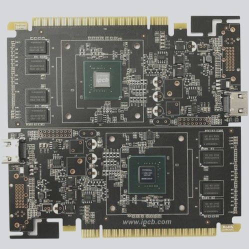
BGA Installation
- Solder paste printing: Use steel plates with trapezoidal openings for easy paste removal without disturbing the printed paste edge. Ensure tin particle size does not exceed 24% of the opening to avoid edge blurring.
- Hot air reflow soldering: Consider particle size and steel plate thickness based on BGA size for optimal soldering results.
Reflow Soldering and PCB Production: Key Considerations
Reflow soldering using forced convection hot air has emerged as the dominant method since the 1990s. The number of heating sections in the production line plays a crucial role in adjusting the “temperature time curve” and increasing production efficiency. For lead-free solders, having more than 10 heating sections is essential, with some processes requiring up to 14 sections.
It is important to note that exceeding the glass transition temperature (Tg) of the PCB and prolonged exposure to high temperatures can result in the board becoming soft and expanding, potentially leading to issues like inner line or plated through-hole (PTH) fractures.
When working with solder paste, the flux must exhibit activity above 130 ℃, with an activity time ranging between 90-120 seconds. Additionally, the heat resistance limit for various components on an FR4 PCB typically averages at 220 ℃, with exposure times not exceeding 60 seconds to prevent damage.