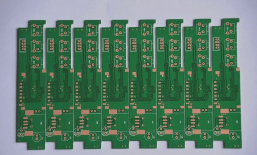
The impedance circuit board’s surface microstrip line features a widely used high characteristic impedance value. Designated as the outer layer’s signal line surface, it utilizes an insulating material to separate it from the adjacent reference surface. The characteristic impedance (Z0) can be calculated using the formula:
Z0=87/SQRT(εr+1.41)×ln[(5.98h)/(0.8w+t)]
Where:
- Z0: Characteristic impedance of the printed wire
- εr: Dielectric constant of the insulating material
- h: Thickness of the medium between the printed wire and the reference surface
- w: Width of the printed wire
- t: Thickness of the printed wire
The main factors influencing characteristic impedance include the dielectric constant (εr), dielectric thickness (h), wire width (w), and wire thickness (t). The relationship between the characteristic impedance circuit board and the substrate material (copper-clad plate) is crucial in PCB design. Minor variations in wire width, thickness, dielectric constant, and insulating medium thickness can lead to changes in characteristic impedance. To control the characteristic impedance effectively, producers must understand the factors affecting its values, master production conditions, and adjust process parameters accordingly within acceptable tolerance ranges to achieve the desired impedance value.

