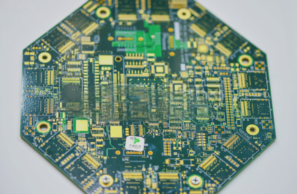
Porosity in Welded Joints and PCB Technology
Porosity is a common issue in welded joints, especially when utilizing PCB technology for reflow solder paste. Large pores (>0.0005 inches/0.01 mm) are often found between LCCC solder joints and PCB solder joints, impacting mechanical properties.
These pores can lead to reduced strength, ductility, and fatigue life of the joint. As pores grow, they may form cracks, contributing to fatigue and increasing stress in the solder, ultimately leading to failure.
The Shanghai SMT chip processing plant has identified solder shrinkage, gas delamination, and entrained flux during soldering as factors contributing to porosity. The complex mechanisms of pore formation in PCB soldering processes involve flux exhaust trapped within the solder during reflow.
Pore formation is influenced by various factors including decreased flux activity, increased metal load of the powder, and the coverage area beneath the lead joint.