Understanding the Impact of Conductor Surface Roughness on PCB Performance
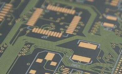
When it comes to PCB production, customers prioritize craftsmanship, price, and timely delivery of PCB boards. The surface roughness of the PCB plays a crucial role in determining the path taken by electromagnetic (EM) waves, which can result in increased signal loss. Higher surface roughness can lead to greater resistance to skin effects, causing a shift in current distribution towards the surface of the conductor during the propagation of EM waves.
Addressing Conductor Surface Roughness in PCB Design
Designers often rely on traditional Morgan Correlation in EM simulators and commercial Computer-Aided Engineering (CAE) tools to tackle the issue of conductor surface roughness. PCB manufacturers adjust surface roughness using numerical factors that are based on smooth-to-rough surface ratios. In the calculation of high-frequency microstrip line loss, the roughness factor (Kr) plays a critical role in matching conductor loss measurements, although discrepancies between actual measurements and computer simulations can sometimes arise.
Minimizing Costly Discrepancies in PCB Performance
Discrepancies between calculated and measured values can prove to be costly during the design stage, often requiring additional iterations to meet performance specifications. Selecting RF PCBs carefully based on conductor surface roughness characteristics can help prevent delays in the design process and ensure optimal performance.
Explore WellCircuits Limited’s PCB Solutions
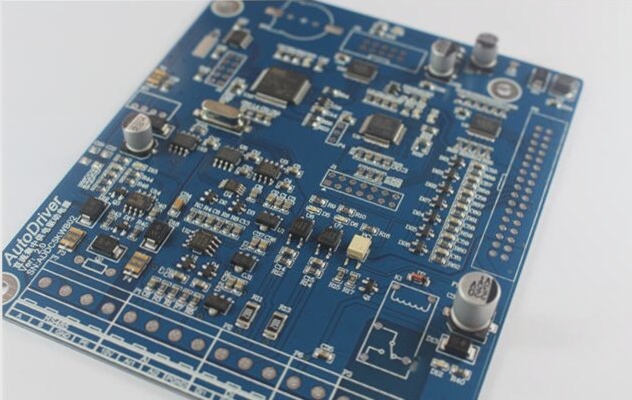
WellCircuits Limited specializes in the production of high-precision double-sided, multi-sided, impedance-controlled, and thick copper circuit boards. Their diverse product range includes HDI boards, backplanes, rigid-flex circuits, buried capacitance and resistance solutions, as well as golden finger boards, catering to a wide range of customer requirements.