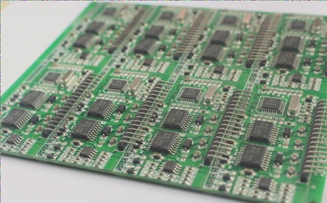
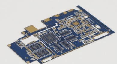
Frequently Asked Questions about PCB Diagram Design by PCB Manufacturers in China
A1: Part Packaging
- Part packaging refers to the appearance and solder joint position of the actual part on the circuit board.
- The part package defines the part’s appearance and solder joint position, allowing different parts to share the same package.
- Part packages can be specified during circuit diagram design or when importing the netlist.

A2: Trace and Flying Wire
- The trace, also known as copper film trace or wire, is crucial for connecting solder joints on the PCB.
- A flying wire is generated by the system based on rules after introducing the netlist to guide the routing.
- A flying wire represents a formal connection without electrical significance, while traces establish electrical connections between solder joints.
A3: Middle Layer vs. Inner Layer
- The middle layer is used for wiring and includes traces, while the inner layer is typically a power supply or ground plane without traces.

A4: External vs. Internal Netlists
- Internal netlists are used for wiring within the PCB system after modifications based on the imported external netlist.
A5: Netlist Introduction Process
- The netlist introduction process involves loading schematic design data into the PCB design system.
- The netlist manager within the PCB system can be used to edit connection relationships between components to form a netlist.