I. Introduction
With the continuous improvement of human requirements for the living environment, environmental issues associated with current PCB board production processes are increasingly prominent. The discussion surrounding lead and bromine is currently heated; the shift towards lead-free and halogen-free materials will significantly influence the future development of PCB boards. While the changes in PCB board surface treatment processes may not seem substantial at present, it is crucial to recognize that gradual shifts over time can lead to profound transformations. As environmental protection concerns amplify, the surface treatment processes of PCB boards are poised for substantial changes in the foreseeable future.
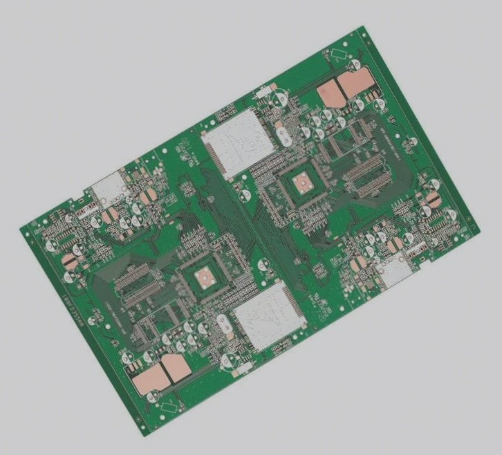
2. The purpose of surface treatment
The fundamental objective of surface treatment is to ensure optimal solderability and electrical properties. Copper, naturally prone to oxidizing in ambient air, requires additional treatments to maintain its integrity. While robust fluxes can eliminate most copper oxides during assembly, their residue is difficult to remove, hence their limited use in industry.
3. Five common surface treatment processes
Numerous surface treatment methods exist for PCB boards. The following are some common ones: hot air leveling, organic coating, electroless nickel plating/immersion gold, immersion silver, and immersion tin, each detailed below.
1) Hot air leveling
Hot air leveling, or hot air solder leveling, involves coating the PCB surface with molten tin-lead solder, then using heated compressed air to flatten it. This forms a protective layer against copper oxidation, ensuring reliable solderability. During this process, copper and tin form a copper-tin intermetallic compound at their interface. Typically, PCBs are immersed in molten solder and then subjected to air-knife treatment to prevent solder bridging. Horizontal hot air leveling is preferred for its uniformity and automation capabilities. The process generally includes micro-etching, preheating, flux coating, tin spraying, and cleaning.
2) Organic coating
Organic coating serves as a barrier between copper and the environment. It is a cost-effective process widely adopted in the industry. Early organic coatings used molecules like imidazole and benzotriazole for rust prevention. Modern coatings, like benzimidazole, chemically bond with copper, allowing for multiple reflow soldering cycles. The process involves degreasing, micro-etching, pickling, pure water cleaning, organic coating application, and final cleaning, offering easier process control compared to other treatments.
3) Electroless Nickel/Immersion Gold
This process deposits a nickel-gold alloy layer on PCB surfaces, providing robust electrical properties and longevity. Unlike organic coatings, it acts as a durable protective layer rather than a simple rust barrier. Nickel prevents gold-copper diffusion, crucial for maintaining performance over time and during lead-free assembly. The complex process includes acid cleaning, micro-etching, pre-dipping, activation, electroless nickel plating, and chemical immersion gold, requiring meticulous process control.
4) Immersion silver
Immersion silver offers simpler and faster application compared to electroless nickel/immersion gold. It provides good electrical performance and storage stability, though lacking the physical strength of nickel-based processes due to the absence of a nickel layer. Silver’s excellent solderability under various conditions makes it suitable for high-frequency signal designs and other applications. The process involves a displacement reaction, resulting in a sub-micron silver coating with added organic compounds to prevent corrosion and migration.
5) Immersion Tin
Immersion tin applies a tin layer compatible with various solder types, addressing issues like tin whisker formation through innovative additives. It forms a flat copper-tin intermetallic compound, ensuring excellent solderability comparable to hot air leveling without its drawbacks. Tin immersion, however, requires careful handling due to its limited shelf life and storage conditions, and the assembly sequence must follow immersion to maintain quality.
6) Other surface treatment processes
Additional methods include electroplated nickel-gold and electroless palladium plating. Electroplated nickel-gold, originating from early PCB surface treatments, involves nickel application followed by gold plating, enhancing solder joint reliability and longevity. Selective electroplating reduces gold usage and improves process control, benefiting applications where solder joint brittleness is a concern. Electroless palladium plating, similar to nickel plating, uses catalytic reduction to deposit palladium for excellent soldering reliability and thermal stability.
4. The choice of surface treatment technology
Selection of surface treatment depends largely on the final assembly’s components and performance requirements. Each process impacts PCB production, assembly, and long-term use differently. The following details specific applications of the five common treatments:
1) Hot air leveling
Once dominant, particularly for larger components, hot air leveling has declined in favor due to its limitations with higher density PCBs and lead-free requirements.
2) Organic coating
Increasingly preferred for its versatility, organic coating suits both low- and high-tech PCBs, particularly where functional surface connections aren’t critical.
3) Electroless Nickel/Immersion Gold
Used extensively for components requiring long-term reliability and electrical performance, though less favored due to solder joint brittleness concerns.
4) Immersion silver
Cost-effective with good electrical properties, suitable for applications requiring reduced costs and good contact reliability.
5) Immersion Tin
Emerging for its compatibility with various solders and avoidance of tin whiskers, ideal for communication backplanes but requiring careful storage and handling.
5. Conclusion
As customer demands rise and environmental regulations tighten, the landscape of PCB surface treatments continues to evolve. The diverse array of available processes reflects ongoing technological advancements and varying application needs, ensuring optimal performance and reliability in modern electronic assemblies.
With the continuous improvement of human requirements for the living environment, environmental issues associated with current PCB board production processes are increasingly prominent. The discussion surrounding lead and bromine is currently heated; the shift towards lead-free and halogen-free materials will significantly influence the future development of PCB boards. While the changes in PCB board surface treatment processes may not seem substantial at present, it is crucial to recognize that gradual shifts over time can lead to profound transformations. As environmental protection concerns amplify, the surface treatment processes of PCB boards are poised for substantial changes in the foreseeable future.

2. The purpose of surface treatment
The fundamental objective of surface treatment is to ensure optimal solderability and electrical properties. Copper, naturally prone to oxidizing in ambient air, requires additional treatments to maintain its integrity. While robust fluxes can eliminate most copper oxides during assembly, their residue is difficult to remove, hence their limited use in industry.
3. Five common surface treatment processes
Numerous surface treatment methods exist for PCB boards. The following are some common ones: hot air leveling, organic coating, electroless nickel plating/immersion gold, immersion silver, and immersion tin, each detailed below.
1) Hot air leveling
Hot air leveling, or hot air solder leveling, involves coating the PCB surface with molten tin-lead solder, then using heated compressed air to flatten it. This forms a protective layer against copper oxidation, ensuring reliable solderability. During this process, copper and tin form a copper-tin intermetallic compound at their interface. Typically, PCBs are immersed in molten solder and then subjected to air-knife treatment to prevent solder bridging. Horizontal hot air leveling is preferred for its uniformity and automation capabilities. The process generally includes micro-etching, preheating, flux coating, tin spraying, and cleaning.
2) Organic coating
Organic coating serves as a barrier between copper and the environment. It is a cost-effective process widely adopted in the industry. Early organic coatings used molecules like imidazole and benzotriazole for rust prevention. Modern coatings, like benzimidazole, chemically bond with copper, allowing for multiple reflow soldering cycles. The process involves degreasing, micro-etching, pickling, pure water cleaning, organic coating application, and final cleaning, offering easier process control compared to other treatments.
3) Electroless Nickel/Immersion Gold
This process deposits a nickel-gold alloy layer on PCB surfaces, providing robust electrical properties and longevity. Unlike organic coatings, it acts as a durable protective layer rather than a simple rust barrier. Nickel prevents gold-copper diffusion, crucial for maintaining performance over time and during lead-free assembly. The complex process includes acid cleaning, micro-etching, pre-dipping, activation, electroless nickel plating, and chemical immersion gold, requiring meticulous process control.
4) Immersion silver
Immersion silver offers simpler and faster application compared to electroless nickel/immersion gold. It provides good electrical performance and storage stability, though lacking the physical strength of nickel-based processes due to the absence of a nickel layer. Silver’s excellent solderability under various conditions makes it suitable for high-frequency signal designs and other applications. The process involves a displacement reaction, resulting in a sub-micron silver coating with added organic compounds to prevent corrosion and migration.
5) Immersion Tin
Immersion tin applies a tin layer compatible with various solder types, addressing issues like tin whisker formation through innovative additives. It forms a flat copper-tin intermetallic compound, ensuring excellent solderability comparable to hot air leveling without its drawbacks. Tin immersion, however, requires careful handling due to its limited shelf life and storage conditions, and the assembly sequence must follow immersion to maintain quality.
6) Other surface treatment processes
Additional methods include electroplated nickel-gold and electroless palladium plating. Electroplated nickel-gold, originating from early PCB surface treatments, involves nickel application followed by gold plating, enhancing solder joint reliability and longevity. Selective electroplating reduces gold usage and improves process control, benefiting applications where solder joint brittleness is a concern. Electroless palladium plating, similar to nickel plating, uses catalytic reduction to deposit palladium for excellent soldering reliability and thermal stability.
4. The choice of surface treatment technology
Selection of surface treatment depends largely on the final assembly’s components and performance requirements. Each process impacts PCB production, assembly, and long-term use differently. The following details specific applications of the five common treatments:
1) Hot air leveling
Once dominant, particularly for larger components, hot air leveling has declined in favor due to its limitations with higher density PCBs and lead-free requirements.
2) Organic coating
Increasingly preferred for its versatility, organic coating suits both low- and high-tech PCBs, particularly where functional surface connections aren’t critical.
3) Electroless Nickel/Immersion Gold
Used extensively for components requiring long-term reliability and electrical performance, though less favored due to solder joint brittleness concerns.
4) Immersion silver
Cost-effective with good electrical properties, suitable for applications requiring reduced costs and good contact reliability.
5) Immersion Tin
Emerging for its compatibility with various solders and avoidance of tin whiskers, ideal for communication backplanes but requiring careful storage and handling.
5. Conclusion
As customer demands rise and environmental regulations tighten, the landscape of PCB surface treatments continues to evolve. The diverse array of available processes reflects ongoing technological advancements and varying application needs, ensuring optimal performance and reliability in modern electronic assemblies.

 العربية
 简体中文
简体中文 Nederlands
 English
 Français
 Deutsch
 Italiano
 日本語
日本語 한국어
한국어 Português
 Русский
 Español
 ไทย
ไทย