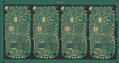
Custom Keyboard PCB Design with USB Hub and USB Type-C Ports
When creating a custom keyboard with integrated USB hub and 2 USB Type-C ports, it’s crucial to consider factors like differential pair routing, matching, and impedance control. With a PCB thickness of 1.6mm and a target of 90ohm differential impedance, precise calculations are essential for track width and spacing.
Key Considerations for PCB Design:
- Ensure proper routing of 7 differential pairs, some spanning over 250mm.
- Optimize component placement and manual routing for connectivity.
- Address challenges without changing board size or opting for a more expensive 4-layer board.
USB Switch Controller and Hub Connection:
The USB switch controller directs traffic between USB-C ports and the hub. Fanout pairs with thinner traces may pose challenges on a 2-layer board.
Track Thickness and Signal Flipping:
Consider the impact of using 0.35mm traces for connections and potential signal flipping on the USB switch to hub link.
Track Transition and Length Matching:
Review track thickness transitions and ensure proper length matching, especially where kinks may leave sections uncoupled.
Optimizing USB-C Port Connections:
Address signal flips and track routing challenges for USB-C ports to enhance signal integrity.
PCB Design Shenanigans: Copper Pour and Signal Integrity
- Considerations for Copper Pours in PCB Design
- Impact of Ground Fill Plane and VCC Fill Plane on Signal Integrity
- Shielding Differential Pairs: Ground vs. Power Distribution
- EMI Concerns and DC Levels in Copper Pour Configurations
- Supporting USB 2.0 Hi-Speed Signals in PCB Layout
- Alternative Methods for Routing Signal Pairs: Twisted Wire Connections
When designing a PCB, the choice of copper pour configuration can have a significant impact on signal integrity. In a recent project, a ground fill plane on the bottom layer and a VCC fill plane on the top layer were used for distributing power to RGB LEDs. While this setup may work for low-power components, it raises questions about differential pair shielding.
Some designers opt for both ground pours to shield the pairs effectively. The theory behind this approach lies in the constant values of the planes, which could maintain a consistent electromagnetic field between them, potentially minimizing signal interference. However, the effectiveness of this method in reducing EMI remains a topic of debate.
It’s crucial to ensure that all signals, especially those supporting USB 2.0 hi-speed signals at 480mbps, are shielded adequately to prevent any signal degradation. In some cases, connecting long signal pairs with twisted wires instead of traditional routing may offer a simpler solution, but the acceptability of this method depends on the specific design requirements.