Faced with a design, there are five crucial attributes to consider when performing EMC analysis of a product and design:
(1) Key device size: This refers to the physical dimensions of the emitting device that produces radiation. The radio frequency (RF) current generates an electromagnetic field that can escape from the housing. The length of the traces on the PCB serves as the transmission path and directly influences the RF current.
(2) Impedance matching: This involves the impedance of both the source and receiver, as well as the transmission impedance between them.
(3) Time characteristics of interference signals: Is the issue a continuous (periodic) event, or does it occur only during specific operations?
(3) Cycle of interference: This could refer to a single event such as a keystroke, power-on noise, periodic disk drive activity, or burst transmissions across a network.
(4) Intensity of the interference signal: This involves assessing the strength of the source’s energy level and its potential to generate harmful interference.
(5) Frequency characteristics of interference signals: Utilizing a spectrum analyzer allows for waveform observation, helping to pinpoint the issue within the spectrum for easier troubleshooting.
Furthermore, attention must be given to certain low-frequency circuit design practices. For instance, while single-point grounding is often favored for low-frequency applications, it can prove unsuitable for RF signal applications, which tend to have increased EMI issues. It is crucial for engineers to recognize that applying single-point grounding indiscriminately across all product designs may lead to more complex EMC challenges.
Current flow within circuit components is another vital aspect. With circuit theory, we understand that current flows from high voltage to low voltage and traverses one or more paths within a closed-loop circuit. Thus, maintaining a small loop is essential. When measuring interfering current, PCB routing may need adjustment to prevent any negative impact on the load or sensitive circuitry. Applications demanding a high impedance path from power to load must take into account all potential return current paths.
Another concern is PCB wiring. The impedance of a wire or trace comprises resistance (R) and inductive reactance. At high frequencies, capacitive reactance is negligible. When wiring frequency exceeds 100 kHz, traces exhibit inductive properties. Wires or traces operating above audio frequencies may inadvertently act as RF antennas. EMC standards dictate that wires or cables should not function below λ/20 of a specific frequency (with antennas typically designed to be λ/4 or λ/2). Unintended designs can result in wires becoming highly efficient antennas, complicating subsequent debugging efforts.
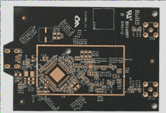
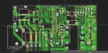
Next, let’s discuss PCB layout. The dimensions of the PCB are crucial; excessively large PCBs can diminish the system’s resistance to interference and increase costs due to extensive wiring. Conversely, overly small PCBs may lead to heat dissipation issues and interference. Additionally, the placement of special components (such as clock components) must be considered—ideally, the clock line should not be routed near key signal lines to minimize interference. Lastly, the overall PCB layout should reflect the circuit’s functionality, ensuring that related components are situated as close together as possible to enhance anti-interference effectiveness.

