Vias are a crucial component in multi-layer PCBs. From a design perspective, a via consists of two primary parts: the central drill hole and the surrounding pad area. The dimensions of these two components determine the overall size of the via. In the PCB manufacturing process, there are five different methods for handling vias: via soldermask opening, via covered with soldermask, via filled with soldermask, via filled with resin, and via filled with copper paste.
Via Soldermask Opening
Via soldermask opening refers to a condition where the via’s pad is left exposed, without soldermask coverage. This process is similar to the one used for plated through-holes for mounting components, where the holes are typically tinned. Via soldermask opening is generally used when the designer requires specific functionalities, such as enabling the via to be measured with a multimeter.
Tip: The effect of via soldermask opening is similar to that of a through-hole. It is unnecessary to disable the Via Window when converting Gerber files.

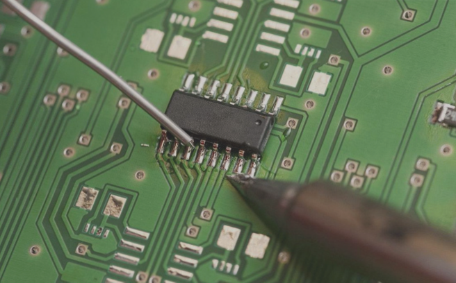
Figure 1. Via Soldermask Opening
Via Covered with Soldermask
Via covered with soldermask refers to the process where the pad of the via is covered with soldermask, preventing it from being exposed. This method is typically used in most circuit boards to ensure optimal electrical performance and to reduce the risk of short-circuiting with other components.
Tip: It is advisable not to design the via hole’s soldermask cover diameter larger than 0.5mm. A larger diameter may result in potential quality issues due to excess soldermask accumulating within the via. When converting PCB design files to Gerber photoplot files, make sure to disable the soldermask opening for vias covered with soldermask to ensure proper coverage.

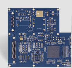
Figure 2. Via Covered with Soldermask
Via Filled with Soldermask
Via filled with soldermask is an extension of the via covered with soldermask process. It involves completely filling the via with soldermask, effectively sealing the via. This helps prevent solder from flowing into the via through the solder mask dams, which could otherwise cause discoloration or “yellowing” of the via. A well-filled via should appear opaque when viewed from one side, meaning it should not be translucent.
Tip: Smaller vias are easier to fill, so it is recommended that vias intended for filling should not exceed 0.5mm in diameter. Larger vias may be difficult to fill completely, leaving the via walls exposed. Additionally, when converting design files to Gerber format for vias filled with soldermask, ensure that the soldermask opening is disabled.

Figure 3. Via Filled with Soldermask
Via Filled with Resin
Via filled with resin refers to the process of filling the inner space of the via with resin, followed by flattening the solder pads through plating. This technique applies to any via with an opening on one side of the board, as well as vias in the center of the board with openings on both sides. The purpose of resin filling can be understood from both a process and design standpoint.
From a process perspective: For blind vias, which are drilled before lamination, failing to fill the holes with resin may result in press-fit PP flowing into the vias during lamination. This can cause delamination and result in voids in the laminate.
From a design perspective: If vias are drilled on the solder pads, not filling the holes with resin before electroplating may lead to insufficient soldering areas, compromising solder quality and potentially affecting the overall reliability of the PCB’s solder joints.
Via Filled with Copper Paste
Via filled with copper paste involves filling the via with high-thermal-conductivity copper paste after plating the hole walls with copper. The filled via is then dried, leveled by grinding, and capped with surface electroplating. This method is suitable for all types of vias, whether they are through-holes with an opening on one side of the board or vias located in the center of the board with openings on both sides.

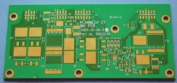
Figure 4. Via Filled with Copper Paste
Differences Between the Five Via Hole Processing Methods
Difference between via covered with soldermask opening and via filled with soldermask: Via covered with soldermask refers to covering the solder pad of a through-hole with soldermask, ensuring complete coverage of the via pad’s outer rim with the green soldermask. Via filled with soldermask involves completely filling the entire via with soldermask, effectively sealing the via and giving it a non-translucent appearance.
Difference between via covered with soldermask and soldermask opening: As mentioned earlier, via covered with soldermask refers to covering the solder pad with soldermask. Soldermask opening, on the other hand, means leaving the solder pad of the via exposed without any soldermask coverage. When surface treatments like tin plating are applied, the exposed via pad functions similarly to a surface-mount pad, allowing the via to be used for soldering components or other interconnections on the PCB.
Difference between via covered with soldermask opening and via filled with soldermask: Soldermask opening leaves the solder pad of the via exposed, allowing light to pass through the via, whereas via filled with soldermask completely seals the via with soldermask, making it opaque and non-translucent.
Difference between via filled with resin and via filled with copper paste: The key distinction lies in the filling materials. For via filled with resin, epoxy resin is used as the filling material, while via filled with copper paste uses copper paste with high thermal conductivity (8 W/m·K) as the filling material.
Note: Due to the inability to distinguish between vias and through-holes in Gerber files, if your files are in Gerber format, we will process them according to your settings in the files.
If you have any questions about PCBs or PCBA, please contact us at info@wellcircuits.com.

