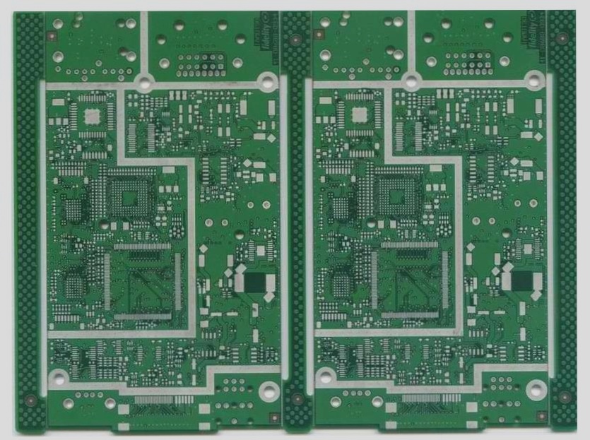
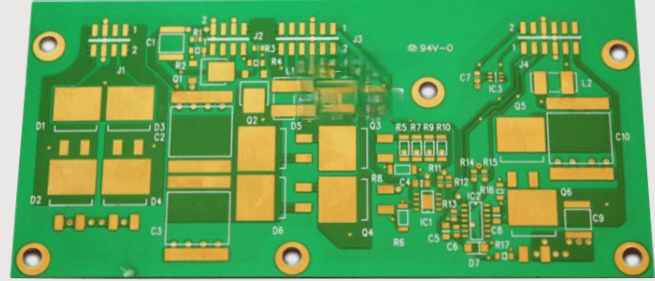
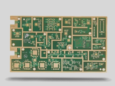
The following is the third operation procedure of solder mask process in the PCB board production process: repairing the board.
Repairing the board includes two aspects: repairing the defects of the image and removing the defects that are not related to the required image. During the repair process, it is important to wear gauze gloves to prevent hand sweat from contaminating the board. Common board defects include:
1. Jumps in the printed lines may be due to excessive electroplating current resulting in thick plating layers, causing the graphic lines to be too high. Additionally, the angle of the squeegee blade and screen printing frame may cause the lines on both sides to be too high, resulting in skip printing. Another reason could be a notched squeegee blade that does not fill in the ink properly, causing skipping. Solutions include controlling the electroplating current and checking for gaps in the squeegee blade.
2. Oxidation may appear as blackening on the copper foil lines under the solder mask of the printed board. This could be caused by inadequate drying of the board after wiping, or splashing of liquid or handprints on the surface before solder mask printing. Visual inspection of the copper foil for oxidation during screen printing is recommended.
3. Uneven surface may occur if the paper is not printed in time during screen printing and residual ink on the screen is not removed, causing an uneven surface. Printing the paper in time to remove residual ink is the solution.
4. Solder mask in the holes could be caused by not printing the paper in time during screen printing, leading to accumulation of residual ink in the screen. Printing the paper in time with a high mesh screen and using high viscosity printing material can help prevent this issue.
5. Pinholes in the graphics may result from dirt on the photographic plate during the exposure process. Regularly checking the cleanliness of the photographic plate during exposure is recommended.
6. Surface dirt can be minimized by ensuring the cleanliness of the clean room where screen printing takes place and implementing measures such as using an electrostatic wire at the screen printing air outlet and maintaining operator cleanliness.
7. Inconsistent colors on both sides of the board may be due to different numbers of knives printed on each side or using a mixture of new and old inks. Avoiding these situations is recommended.
8. Cracking on the board surface could occur due to insufficient exposure during the exposure process. Ensuring the exposure parameters are within the appropriate range can prevent cracking.
9. Bubbles between lines or on single lines may be caused by narrow line spacing and high lines, preventing proper printing of the solder mask on the substrate. Visually checking the screen printing material and controlling the electroplating current can help prevent bubbles.
10. Ghosting, regular ink dots next to pads on the board, may result from improper board positioning during screen printing and not removing residual ink on time. Firmly fixing the paper with positioning pins and timely removal of residual ink can resolve this issue.
In cases where defects cannot be repaired, using a sodium hydroxide aqueous solution to dissolve the original solder resist and re-screen printing and exposure is necessary. Small defects like a small copper dew point can be carefully repaired with a fine brush and adjusted solder mask.


