In the rapidly evolving world of electronics, flex PCB fabrication has emerged as a critical process, enabling the creation of innovative and highly functional electronic devices. Flexible printed circuit boards (PCBs) offer unparalleled flexibility, compactness, and reliability, making them ideal for a wide range of applications. This article provides a detailed overview of flex PCB fabrication, including its process, applications, and the latest trends in the industry.

Understanding Flex PCB Fabrication
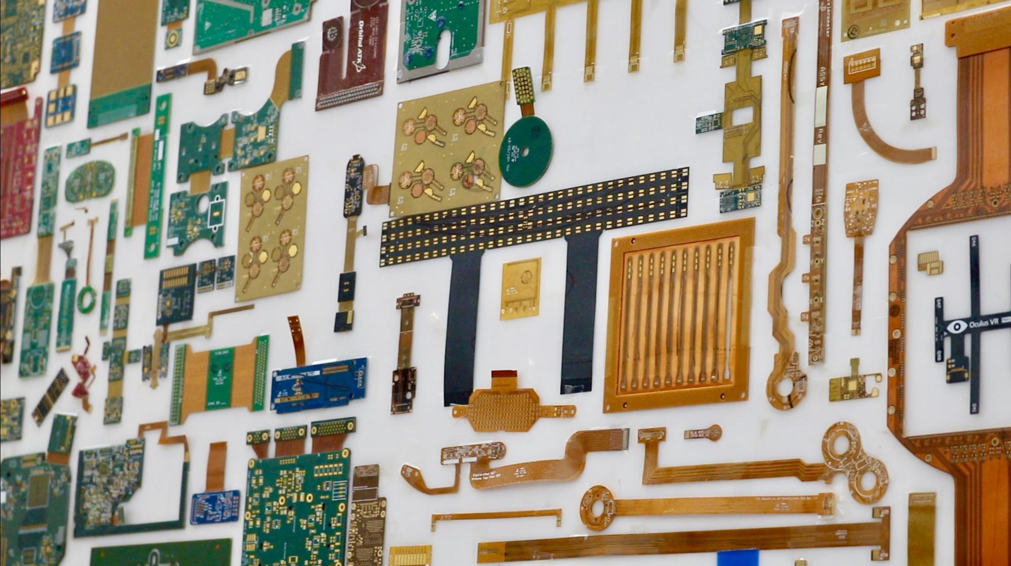
Flex PCB fabrication involves a series of specialized processes designed to create circuit boards that can bend, twist, or fold without compromising functionality. These boards are crucial in applications where space, weight, and reliability are critical factors, such as aerospace, automotive, medical devices, and wearable technology.

Key Stages in Flex PCB Fabrication
- Design and Specification
The journey of flex PCB fabrication begins with the design phase. Engineers use specialized software like Altium Designer, Eagle, or KiCAD to create the circuit layout. This step defines the geometry, number of layers, and required specifications of the flex PCB. Designers also need to account for mechanical features such as bend areas, where the board will be flexible. - Material Selection
One of the key advantages of flex PCBs is the use of flexible materials. Polyimide (PI) is a popular choice due to its excellent thermal stability and flexibility. Other materials, like polyester (PET), are used for certain types of applications. The choice of material directly impacts the board’s flexibility, durability, and performance. - Copper Cladding
The next step involves applying copper cladding to the base substrate. This is done by bonding a thin layer of copper to the polyimide or other flexible material using a special adhesive. This copper will form the electrical pathways that connect various components on the board. - Photolithography
In this step, the copper-coated substrate is exposed to UV light through a photomask. The photomask contains the circuit design, which is transferred onto the copper layer. This process defines the areas of copper that need to remain on the flex PCB. - Etching
Once the design is transferred onto the copper, an etching solution removes the unwanted copper from the board, leaving behind only the traces that form the circuit. This is a critical step to ensure that the electrical pathways are clear and precise. - Developing
After etching, the board is developed to remove the remaining photoresist layer that protected the copper traces during exposure. This step leaves behind the final copper pattern, ready for the next phase of flex PCB fabrication. - Drilling
To create vias (electrical pathways between different layers) and holes for components, the flex PCB undergoes a drilling process. This step is especially critical for multilayer flex PCBs that require precision in hole placement for correct assembly. - Plating
After drilling, the vias and holes are plated with copper to ensure proper conductivity. This is done by electroplating, which deposits a thin layer of copper into the drilled holes. - Impedance Control
For high-speed applications, impedance control is crucial. Designers ensure that the flex PCB maintains the correct impedance for signal integrity. This is often done by adjusting the copper trace width or modifying the stack-up configuration. - Lamination
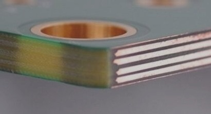
The flex PCB is then laminated to fuse the copper traces with the base substrate and provide additional strength to the board. For multilayer flex PCBs, this step is repeated to bond each layer together, creating a stack of flexible layers. - Solder Mask Application
A solder mask is applied to the flex PCB to protect the copper traces from corrosion, improve solderability, and prevent short circuits during assembly. The solder mask also ensures that only the necessary areas are exposed for component attachment. - Silkscreen Printing
Silkscreen printing is used to add markings, labels, or component designators to the flex PCB. These markings help with component placement and assembly and provide necessary information for troubleshooting during the operational phase. - Bend Testing
One of the most unique aspects of flex PCB fabrication is its flexibility. During bend testing, the board is subjected to bending cycles to ensure it can withstand the stresses of its intended application. A well-designed flex PCB can endure up to 200,000 bending cycles without failure. - Cutting and Shaping
After all layers are bonded, the flex PCB is cut and shaped to the final specifications. This step ensures that the board fits into the device or system for which it was designed, whether it’s a wearable or a complex industrial machine. - Surface Finish
To improve the solderability and reduce the risk of oxidation, a surface finish such as HASL (Hot Air Solder Leveling), ENIG (Electroless Nickel Immersion Gold), or OSP (Organic Solderability Preservative) is applied to the copper pads. This is especially important for flex PCBs that will be soldered during assembly. - Component Placement and Soldering
Once the flex PCB is ready, components are placed on the board either manually or by automated pick-and-place machines. The components are then soldered to the pads, completing the electrical connections required for the device. - Inspection and Testing
Each flex PCB undergoes rigorous inspection and testing. This includes visual checks, automated optical inspection (AOI), and electrical testing to ensure that the board meets all functional specifications and there are no defects. - Packaging and Delivery
Once the flex PCB has passed all tests, it is packaged carefully to avoid any damage during shipping. For customers like PCBONLINE, this includes providing clear instructions and labeling to ensure that the flex PCB arrives ready for assembly. - Post-Fabrication Modifications
Depending on the application, additional post-fabrication modifications might be required. This could involve attaching stiffeners, transparent overlays, or thermal management solutions to enhance the board’s performance. - Final Quality Assurance
Before the flex PCB reaches the customer, a final quality assurance (QA) check is performed. This step ensures that the board adheres to all specifications, such as size, function, and electrical performance.
Advantages and Applications of Flex PCBs
Flex PCBs offer several advantages over rigid PCBs, making them ideal for diverse applications:
- Space and Weight Reduction: Their thin, lightweight nature allows for compact designs and reduced overall product weight.
- Enhanced Reliability: Flex PCBs exhibit better resistance to mechanical stress, vibration, and thermal expansion, which is crucial for applications subjected to harsh environmental conditions.
- Design Flexibility: The ability to bend or twist enables designers to create innovative product shapes and configurations that are not feasible with rigid boards.
- Cost Efficiency: Despite initial higher material costs, flex PCBs often reduce overall assembly and maintenance costs due to simplified interconnection and reduced need for additional components.
Flex PCBs find extensive use in various industries:
- Consumer Electronics: Mobile devices, tablets, and wearable technology benefit from the compact and durable nature of flex PCBs.
- Automotive: In-car electronics, sensors, and control systems leverage flex PCBs for space-saving and reliability in challenging automotive environments.
- Medical Devices: Flexible circuits are crucial in medical equipment and implants where biocompatibility and reliability are paramount.
- Aerospace and Defense: Satellite systems, UAVs, and military applications rely on flex PCBs for lightweight, reliable performance in extreme conditions.
Challenges in Flex PCB Fabrication
While flex PCBs offer significant advantages, their fabrication presents unique challenges:
- Complex Manufacturing Process: The intricate processes involved in flex PCB fabrication require specialized equipment and expertise, increasing production complexity and costs.
- Handling and Assembly: Flex circuits must be handled with care during assembly to prevent damage to delicate components and circuitry, especially around bends and folds.
- Material Compatibility: Selecting compatible materials and adhesives is crucial to ensure reliability and performance under varying environmental conditions.
Conclusion
Flex PCB fabrication represents a critical advancement in electronics manufacturing, enabling innovative designs and reliable performance across diverse industries. As technology continues
WellCircuits offers FLEX PCB RIGID-FLEX PCB and PCBA manufacturing services for 1 to 32 layers. For more details, please refer to our PCB manufacturing and PCBA Manufacturing.
If you have any PCB or PCBA RFQ, please send it to info@wellcircuits.com


