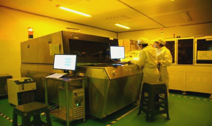
Flexible circuit manufacturing involves far fewer fabrication steps compared to rigid PCBs, so let’s briefly introduce them.
1. Adhesive/Seed finishing: Either an epoxy or acrylic adhesive is used, or sputtering is used to create a thin copper layer for a plating key.
2. Copper foil added: Copper foil is included, either by lamination to the glue (the more mainstream approach) or chemical plating onto the seed layer. Newer construction processes by products suppliers allow for adhesiveless lamination of rolled stiff copper as an option.
3. Drilling: Openings to vias and pads are frequently mechanically pierced. Several plated flex substrates can be drilled concurrently by incorporating them from several reels on drums, exploration in between working plates, after that rolling out to separate reels on the other side of the drilling maker. Pre-cut flex panels can be combined as well as pierced between rigid blanks similarly inflexible cores are pierced too, though it calls for more careful registration and the alignment accuracy is reduced. For ultra-small openings, laser drilling is readily available, though at a lot included cost due to the fact that each film needs to be drilled independently. This would certainly make use of Excimer (ultraviolet) or YAG (Infrared) lasers for higher accuracy (microvias), as well as CO2 lasers for medium openings (4+ mils). Huge openings and also cut.
4. Through-hole plating: When the holes are made, copper is transferred and also chemically plated similarly as stiff PCB cores. (typically referred to as Cuposit). Through-hole layering in flex circuits is suggested to be at the very least 1 mil in layering density to add mechanical support to the pad or through, whereas a typical low-cost rigid PCB may just have 1/2 mil cuposit.
5. Etch-resist printing: Photosensitive etch resist is coated onto the film surfaces, and the desired mask pattern is used to reveal and establish the resist before chemical etching of the copper.
6. Etching and stripping: After exposed copper is etched, the etch resist is chemically removed from the flex circuit.
7. Coverlay or Covercoat: Top and bottom sections of the flex circuit are protected by coverlay layers which are cut to shape. There may be components actually installed on sections of the flexible circuit, in which case the coverlay is also acting as a solder mask. The most common coverlay material is additional polyimide film with adhesive though adhesiveless processes are available. In the adhesiveless process, photoimageable solder mask (the same as used on rigid board sections) is used essentially printing the coverlay onto the flex circuit. For coarser cheaper designs screen printing is also an option with final hardening of this cover coat film by UV exposure. Essentially, the difference is that coverlay is a laminated film, whereas covercoat is a applied material coating which then needs to be cured.
8. Cutting out the flex: The final step in creating the flex circuit is cutting it out. This is usually referred to as “blanking”. The high-volume cost-effective approach to blanking is by a hydraulic punch and die set which includes relatively high tooling costs. However, this method permits punching out of many flex circuits at the same time. For prototype and low-volume runs, a blanking knife is used. The blanking blade is essentially a long razor blade, bent into the shape of the flex circuit outline and fastened into a guided slot in a support board (MDF, plywood or thick plastic such as teflon). The flex circuits are then pressed into the blanking blade to be cut out. For even smaller prototype runs, X/Y cutters (similar to those used in vinyl sign making) could be used.

1. This is a 1100mm length flex PCB made of polyimide material with ENIG.
2. WellCircuits.com is a leading manufacturer of long flexible circuits and Polyimide Flex PCBs in China, specializing in meeting your demand for flexible printed circuit boards.

1. WellCircuits specializes in manufacturing a 10-layer flexible PCB, specifically designed for high-quality flex PCB connectors.
2. Our expertise lies in both multilayer flexible PCB prototyping and mass production.
3. We offer a variety of materials, including LCP, Dupont Kapton, Pyralux, and Panasonic FELIOS, to meet the specific needs of our customers.

specialize in quick-turn flexible PCB prototyping to meet the fast-paced demands of the electronics industry. Our team of experts and state-of-the-art facilities enable us to deliver high-quality flex PCB prototypes with short lead times. From single-sided to multi-layer flex PCBs, we have the capabilities to bring your designs to life. We understand the importance of fast prototyping in the development process, and our goal is to help our clients accelerate their time to market. Whether you are a small startup or a large corporation, we are committed to providing the best flex PCB prototyping solutions to meet your unique needs. Contact us today to learn more about our flexible PCB prototyping services.

1. WellCircuits Ltd offers a comprehensive FPC+Component sourcing+ assembly service to global customers, serving as a one-stop solution for all your needs.
2. Our flexible PCB assembly services encompass both SMT and DIP, providing a complete solution for your requirements.
3. If you are in need of a quick-turn flexible PCBA service provider, do not hesitate to contact us at your earliest convenience. You can reach us by phone at [phone number] or via email at [email protected].

1. As a PCB expert, I can help you with the following revised and polished article:
2. A double-sided flexible PCB prototype created by WellCircuits.com, featuring a 3u” Electroplated Gold finish. Do you need a quote for a similar flex PCB? Contact us today! We are a professional flex PCB manufacturer based in China.

1. High density interconnected (HDI) PCBs represent one of the fastest-growing technologies in the PCB industry.
2. Due to their higher circuitry density compared to traditional circuit boards, HDI PCB designs are capable of incorporating smaller vias, capture pads, and higher connection pad densities.

