The PCB Fabrication Process
- Adjusting Image Contrast and Brightness: Start by adjusting the canvas contrast and brightness in PHOTOSHOP to distinguish areas with copper film. Convert the image to black and white and ensure clear lines. Save as TOP1.BMP and BOT1.BMP.
- Converting to PROTEL Format: Convert the BMP files to PROTEL format and import them as separate layers. Align PAD and VIA positions; repeat if needed.
- Converting to PCB Files: Convert TOP1.BMP and BOT1.BMP to TOP1.PCB and BOT1.PCB, including the SILK layer. Trace components and delete SILK layer after tracing.

Inner Copy Board Process
- Scanning the Inner Layer: Remove surface layers of the circuit board, clean off silk screen and solder mask, and scan TOP LAYER and BOTTOM LAYER separately in color.
- Drawing the Inner PCB Board: Enhance contrast in PHOTOSHOP, convert to black and white, save as TOP2.BMP and BOT2.BMP. Convert to PROTEL format, trace lines, place devices, and delete SILK layer.
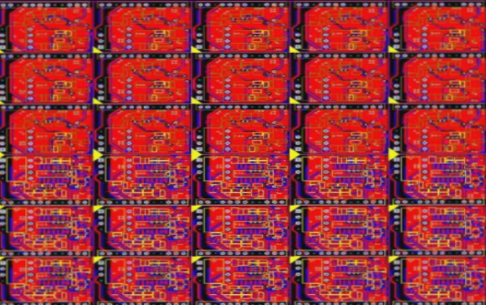
- Combining Layers and Printing: Import files into PROTEL, combine images, print on transparent film, and check for errors.
Synthetic Four-Layer Board
Combine surface and inner layer images into a PCB file, completing the four-layer motherboard copying process. Export the PCB file for board production and component soldering to finalize the circuit board cloning.


