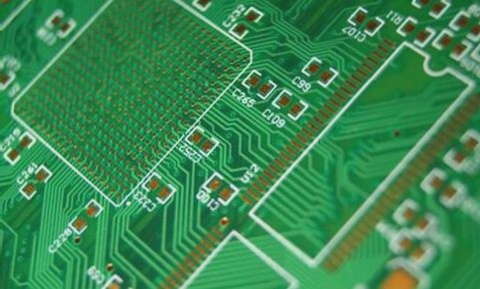
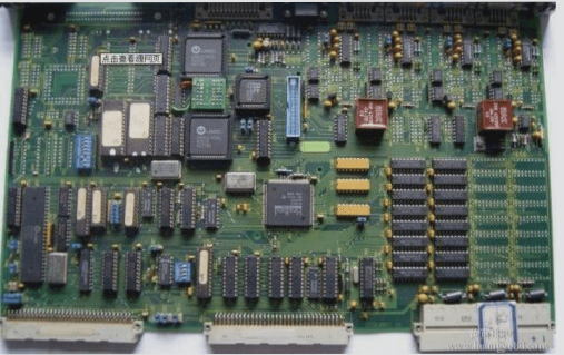
1. **Finger Row Electroplating:**
Circuit board production often requires rare metals to be plated on edge connectors, edge protruding contacts, or gold fingers to provide lower contact resistance and higher wear resistance. This technique is called finger row plating or protruding part plating. Gold is often plated on the protruding contacts of the board edge connector with a nickel inner plating layer. The gold fingers or the protruding parts of the board edge are plated manually or automatically. Currently, gold plating on the contact plug or gold finger is typically done using a plating or lead method, rather than plated buttons. The process is as follows:
1) Strip the coating to remove the tin or tin-lead coating on the protruding contacts
2) Rinse with washing water
3) Scrub with abrasives
4) Activate by diffusion in 10% sulfuric acid
5) Nickel plating thickness on the protruding contacts is 4 -5μm
6) Clean and demineralize with water
7) Gold penetration solution treatment
8) Gold plating
9) Cleaning
10) Drying
2. **Through-Hole Plating:**
There are numerous methods to apply an electroplating layer on the entire wall of a substrate’s drilled hole. This process, known as hole wall activation in industrial applications, requires multiple intermediate storage tanks in the commercial production process of printed circuits, each with its own control and maintenance requirements. Through-hole plating is an essential follow-up process to the drilling phase. As the drill bit penetrates the copper foil and substrate below, the heat generated melts the insulating synthetic resin, primarily composing the substrate matrix. The molten resin and other drilling debris accumulate around the hole, coating the newly exposed hole wall in the copper foil. However, this accumulation is detrimental to subsequent electroplating. The molten resin also leaves a layer on the entire wall of the substrate, exhibiting poor adhesion to most activators. Hence, a class of similar de-staining and etch-back chemical technologies needs development.
A more suitable method for prototyping printed circuit boards is to utilize specially designed low-viscosity ink to form a high-adhesion, high-conductivity film on the inner wall of each through-hole. With this approach, multiple chemical treatment processes are unnecessary, requiring only one application step, followed by thermal curing, to form a continuous film on the inner side of all hole walls. This film can be directly electroplated without further treatment. The ink, a resin-based substance, exhibits strong adhesion and can easily adhere to the walls of most thermally polished holes, eliminating the need for etch-back.


![Could you please explain the concept of a resistive circuit?”]](https://cdn.wellcircuits.com/wp-content/uploads/2024/07/2e309995bb3d906ac889b9bf4a0c2f99.jpg)