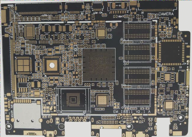
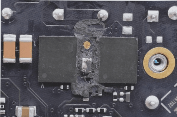
There are numerous approaches to addressing PCB-based product design challenges, each with significant differences. But which method is the quickest? Which is the most efficient? Which project requires the least resources? All these factors greatly influence the project’s success. For PCB designers, two paths are available: First, you can create a design without constraints and then seek out a production chain to realize it. The second option involves understanding your production chain and tailoring your design to leverage the manufacturer’s strengths while still achieving the necessary functionality.
Senior designers share five strategies here that can help you plan effectively without adding weeks or unnecessary costs to the design process.
1. Research and select suppliers early in the design.

1. After the design team completes the prototype design, the subsequent step in the process is to acquire a prototype design processing example for testing. While this may seem like a mere planned step for the team, it actually involves several phases, such as purchasing components and fabricating printed circuits. These components must be properly connected to the PCB. The realization of the entire production process hinges on the selection and management of the design team. Thus, it’s crucial to grasp the production process beforehand, including component availability and service provider capabilities, which can significantly reduce rework and redesign. Know thyself, ever-victorious. Ultimately, the printed circuit board must be manufactured according to the design.
2. Before layout, focus on reducing costs and optimizing performance. Cost considerations extend beyond the number of components used in the design; they also encompass the complexity of the PCB design, the number of flying probe tests, and any design-related manufacturing issues. Therefore, it’s essential to optimize PCB performance comprehensively before layout, minimizing unnecessary cost investments as much as possible.
3. Shape your layout into a “sweet spot” for the manufacturing plant. Regardless of the manufacturer selected, there will be a “sweet spot,” with the design positioned within the manufacturing process window. From this perspective, small manufacturing adjustments within production capacity can maintain the integrity of your design, thus enhancing profitability and reliability.
4. Utilize supplier DFM tools to assess your layout’s production capacity. A reputable PCB manufacturer will run your design through a design for manufacturing (DFM) tool to identify any visual inspection errors. A top-tier manufacturer will provide a feasibility report when quoting your design, verifying its suitability for the manufacturing process. This report is a critical step in securing an appropriate assembly board and represents the first measure in developing optimized production circuit boards. When PCB designs are simpler or significantly aligned with current technological advantages, these strategies may have a lesser impact on your design cycle. However, if the requirements for circuit testing errors are stringent, these strategies become increasingly vital.


 العربية
 简体中文
简体中文 Nederlands
 English
 Français
 Deutsch
 Italiano
 日本語
日本語 한국어
한국어 Português
 Русский
 Español
 ไทย
ไทย