4 Types of Surface Treatments for PCB Circuit Board Prototyping
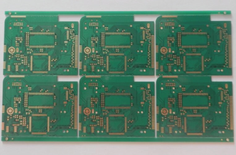
Different PCB factories employ various surface treatment methods during circuit board prototyping. Each surface treatment method has its own distinct characteristics. Taking chemical silver as an example, the process is relatively straightforward. It is especially recommended for lead-free soldering and SMT, particularly for applications requiring fine circuit patterns. The key advantage of using chemical silver as a surface treatment is that it significantly reduces overall costs, making it a cost-effective choice. In this article, we will introduce several common surface treatment methods for PCB prototyping.
1. **HASL (Hot Air Solder Leveling) – Tin Plating**
Tin plating is a traditional method used in PCB prototyping. It is now available in two variants: leaded tin and lead-free tin. The advantages of tin plating include: after the PCB is completed, the copper surface is fully wetted (the tin completely covers the surface before soldering). This makes it suitable for lead-free soldering. The process is mature, cost-effective, and well-established. Additionally, it is ideal for visual inspection and electrical testing, making it one of the most reliable and widely-used methods for PCB prototyping.

2. **Chemical Nickel Gold**
Nickel gold is a widely used PCB surface treatment process for prototype manufacturing. It is important to note that the nickel layer is actually a nickel-phosphorus alloy. Depending on the phosphorus content, it is categorized into high-phosphorus and medium-phosphorus nickel, which have different applications that will not be discussed here. The advantages of nickel gold include: compatibility with lead-free soldering; a very smooth surface, making it ideal for SMT; suitability for electrical testing; design flexibility for switch contacts; applicability for aluminum wire bonding; effectiveness for thick PCBs; and strong resistance to environmental factors.
3. **Electroplated Nickel Gold**
Electroplated nickel gold can be classified into “hard gold” and “soft gold.” Hard gold, often a gold-cobalt alloy, is commonly used on gold fingers (contact areas), while soft gold is pure gold. Electroplated nickel and gold are widely used on IC substrates, such as PBGA, primarily for bonding gold and copper wires. The IC substrate is suitable for electroplating, but the gold finger areas require additional conductive wiring for plating. The key advantages of electroplated nickel-gold in PCB prototyping are: its suitability for contact switch designs, gold wire bonding, and electrical testing.
4. **Nickel Palladium**
Nickel-palladium-gold is an emerging surface treatment in PCB prototyping, though it has been more commonly used in the semiconductor industry. It is especially suitable for gold and aluminum wire bonding. The benefits of using nickel-palladium-gold for PCB prototyping include its application on IC carrier boards, suitability for both gold and aluminum wire bonding, and compatibility with lead-free soldering. Compared to ENIG, nickel-palladium-gold eliminates the risk of nickel corrosion (black pad issues) and is more cost-effective than ENIG and electroplated nickel gold. It is suitable for a variety of surface treatment processes and applications on PCBs.
If you have any PCB manufacturing needs, please do not hesitate to contact me.Contact me