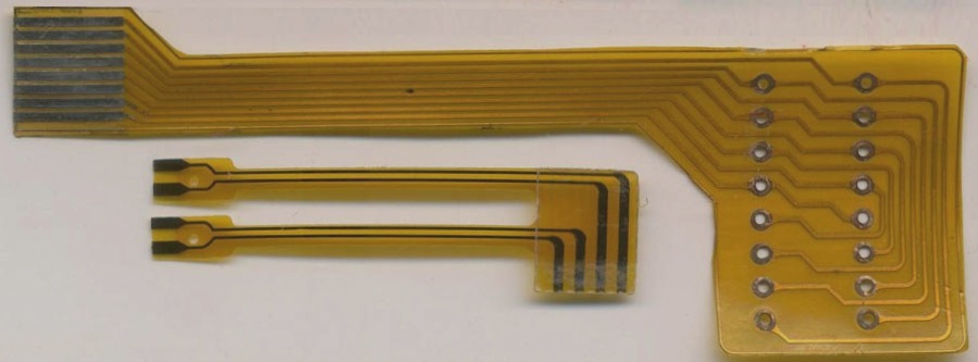
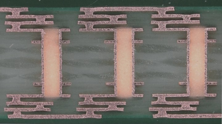
The basic process of the FPC photocoating layer is similar to the photoresist film used in rigid printed boards. The materials used can be dry film type or liquid ink type. However, solder mask dry film is still different from liquid ink. While the coating process for dry film and liquid ink types is different, the same equipment can generally be used for exposure and subsequent processes with some adjustments. Specific process conditions will vary.
For dry film, it must be applied first, covering all circuit diagrams. The typical dry film method may result in air bubbles between lines, so a vacuum filming machine is used. Ink type involves coating the circuit pattern using screen printing or spraying methods. Screen printing is a common method, similar to rigid printed board processes. However, if the ink coating is too thin or uneven, a second printing may be necessary to improve reliability.
Spraying is a newer technology that offers adjustable thickness and uniform coating, suitable for mass production. Epoxy resin and polyimide are common ink types for screen printing, requiring mixing with curing agent before use. Solvents can be added to adjust viscosity, and drying is necessary after printing. Double-sided circuits require coating and drying on both sides for proper curing.
Pattern exposure of the photocoating layer requires precision in positioning. If the size of the disk is around 100um, the covering layer’s accuracy should be at least 30-40um. Achieving this precision depends on the device’s mechanical capabilities. However, size expansion or deformation in flexible printed boards may make meeting higher accuracy requirements challenging.
Developing the pattern should be done carefully, with attention to developing conditions. Sodium carbonate aqueous solutions are commonly used as developers. Avoid using the same developer for pattern development, especially in small batch production. Post-curing is essential to fully cure the developed photocoating layer resin, with curing temperatures and times varying depending on the resin type. A curing oven is typically used for 20-30 minutes.