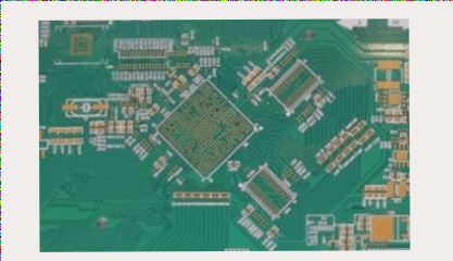
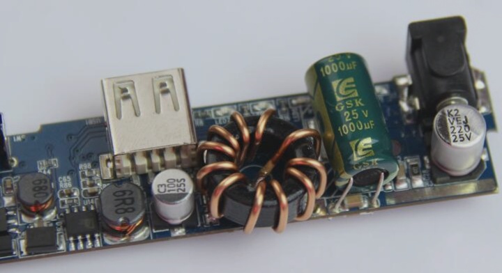
The understanding of PCB wiring and routing is quite sophisticated; each expert brings their own experiences, yet certain fundamental principles remain consistent.
◆ Traces for high-frequency digital circuits should be thinner and shorter.
◆ It is crucial to maintain isolation between high-current signals, high-voltage signals, and small signals (the isolation distance correlates with the required withstand voltage. Typically, a spacing of 2mm is needed for 2KV, with distances increasing proportionally. For instance, to withstand a 3KV voltage test, the separation between high and low voltage lines should exceed 3.5mm. In many cases, slots are also created on the PCB to prevent creepage between high and low voltage areas.)
◆ When connecting two panels, the wires on either side should be arranged perpendicularly, diagonally, or bent to avoid running parallel, thereby minimizing parasitic coupling. It’s best to limit the use of printed wires as circuit inputs and outputs. To prevent feedback, placing a ground wire between these lines is advisable.
◆ Routing corners should ideally exceed 90 degrees; avoid angles below 90 degrees, and minimize the use of 90-degree turns.
◆ For identical address or data lines, trace lengths should not vary significantly; otherwise, shorter traces may need to be artificially bent for compensation.
◆ Traces should be placed on the soldering surface whenever possible, especially in through-hole PCBs.
◆ Limit the use of vias and jumpers as much as possible.
◆ Single-sided PCB pads should be sufficiently large, with thick connections to the pads; teardrops should be employed where feasible. Generally, the quality of single-sided PCBs can be inconsistent, which may lead to soldering issues and rework.
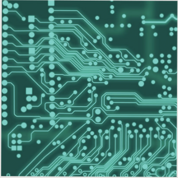
◆To prevent bubbles and board bending due to thermal stress during wave soldering, a large copper area should be covered with a grid. However, in specific cases, the flow direction and size of the GND must be carefully considered; it cannot simply be filled with copper foil, but should be properly routed.
◆Components and traces should be positioned away from the edges. Typically, single-sided boards are made of paper materials, which are prone to breaking under stress. Placing connections or components near the edges can lead to issues.
◆The convenience of production, debugging, and maintenance should be prioritized.
For analog circuits, addressing ground issues is crucial. Ground noise can be unpredictable and, once generated, can cause significant problems. For power amplifier circuits, even minimal ground noise can greatly affect sound quality due to amplification; in high-precision A/D conversion circuits, high-frequency components on ground wires can cause temperature drift, impacting amplifier performance. To mitigate this, decoupling capacitors can be added at the board’s four corners, with one pin connected to the board’s ground and the other to the mounting hole (secured by screws), ensuring stability for both the amplifier and A/D converter.
Moreover, electromagnetic compatibility is increasingly vital as focus shifts to environmentally friendly products. There are generally three sources of electromagnetic signals: the signal source, radiation, and transmission lines. Crystal oscillators are common high-frequency signal sources, with each harmonic’s energy value significantly exceeding the average. Effective strategies include controlling signal amplitude, grounding the crystal housing, shielding interference signals, and employing specialized filter circuits and devices.
A special note on serpentine traces is necessary, as their function varies based on application. They are used for clock signals on computer motherboards, such as PCIClk and AGP-Clk, serving two primary purposes: 1. Impedance matching, and 2. Filtering inductance.
For critical signals like HUBLink in the INTELHUB architecture, there are 13 signals that can reach frequencies of 233MHz, requiring precise length matching to eliminate timing issues. In this context, serpentine routing is essential.
Typically, the spacing of serpentine traces should be at least twice the line width; when used on standard PCBs, they can also function as inductive coils for radio antennas, in addition to serving as filter inductors.

