1. Usually, a printed circuit board, which is a printed component or a conductive pattern made from a combination of both, is constructed on an insulating material according to a predetermined design and is referred to as a printed circuit.
2. A conductive pattern that provides electrical connections between components on an insulating substrate is known as a conductive pattern. This is also considered part of the printed circuit.
3. The term “printed circuit board” (Printed Circuit Board, PCB), or simply “printed circuit board,” is used to describe this assembly.
4. The substrate of the printed circuit board is made from insulating and heat-resistant materials that are not easily bendable.
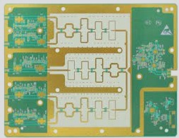
5. The small traces visible on the surface are made of copper foil.
6. Initially, the copper foil covers the entire board, but parts of it are etched away during the manufacturing process, leaving behind a network of small traces.
7. These traces, known as wires or wiring, provide the necessary circuit connections for the components on the PCB.

1. PCB is used in virtually all types of electronic equipment, including electronic toys, mobile phones, and computers. As long as electronic components like integrated circuits are present, PCBs facilitate electrical interconnection between them.
2. PCB Composition
A complete PCB consists of the following five main parts:
– Insulation base material: Typically made from phenolic paper, epoxy paper, or epoxy glass cloth.
– Copper foil surface: The core of the PCB, comprising exposed pads and copper foil circuits covered by green solder mask. Pads are used for component soldering.
– Solder mask: Protects the copper foil circuits and is made from high-temperature resistant solder resist.
– Character layer: Marks the numbers and symbols of components for easy circuit identification during PCB processing.
– Holes: Facilitate substrate processing, component installation, product assembly, and connections between copper foil circuits at different layers.
3. The green or brown on the PCB represents the color of the solder mask. This insulating layer protects the copper traces and prevents incorrect component soldering. Additionally, a screen-printed layer, often white, marks component positions and is referred to as the icon layer.
4. Function of PCB
– Provide mechanical support: PCBs support and secure various electronic components, such as integrated circuits, during assembly.
– Realize electrical connection or insulation: PCBs ensure both electrical connections and insulation between electronic components.
– Additional functions: PCBs offer solder mask graphics for automatic assembly and provide identification and graphics for component insertion, inspection, and maintenance.
5. This concludes the introduction to the basic structure and functions of PCBs.
2. A conductive pattern that provides electrical connections between components on an insulating substrate is known as a conductive pattern. This is also considered part of the printed circuit.
3. The term “printed circuit board” (Printed Circuit Board, PCB), or simply “printed circuit board,” is used to describe this assembly.
4. The substrate of the printed circuit board is made from insulating and heat-resistant materials that are not easily bendable.
5. The small traces visible on the surface are made of copper foil.
6. Initially, the copper foil covers the entire board, but parts of it are etched away during the manufacturing process, leaving behind a network of small traces.
7. These traces, known as wires or wiring, provide the necessary circuit connections for the components on the PCB.

1. PCB is used in virtually all types of electronic equipment, including electronic toys, mobile phones, and computers. As long as electronic components like integrated circuits are present, PCBs facilitate electrical interconnection between them.
2. PCB Composition
A complete PCB consists of the following five main parts:
– Insulation base material: Typically made from phenolic paper, epoxy paper, or epoxy glass cloth.
– Copper foil surface: The core of the PCB, comprising exposed pads and copper foil circuits covered by green solder mask. Pads are used for component soldering.
– Solder mask: Protects the copper foil circuits and is made from high-temperature resistant solder resist.
– Character layer: Marks the numbers and symbols of components for easy circuit identification during PCB processing.
– Holes: Facilitate substrate processing, component installation, product assembly, and connections between copper foil circuits at different layers.
3. The green or brown on the PCB represents the color of the solder mask. This insulating layer protects the copper traces and prevents incorrect component soldering. Additionally, a screen-printed layer, often white, marks component positions and is referred to as the icon layer.
4. Function of PCB
– Provide mechanical support: PCBs support and secure various electronic components, such as integrated circuits, during assembly.
– Realize electrical connection or insulation: PCBs ensure both electrical connections and insulation between electronic components.
– Additional functions: PCBs offer solder mask graphics for automatic assembly and provide identification and graphics for component insertion, inspection, and maintenance.
5. This concludes the introduction to the basic structure and functions of PCBs.


