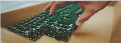
PCB Blanking and Shape Processing Techniques
Blanking of printed circuit boards, which includes creating holes and shapes, can be achieved through die punching. This method is particularly suitable for manufacturing low-profile PCBs in small or large quantities, providing cost-effective solutions.

Punching Process
- One or several dies are used to create single-sided paper substrates with complex shapes and numerous holes.
- Epoxy glass cloth substrates with double-sided non-metallized holes can also be produced using punching.
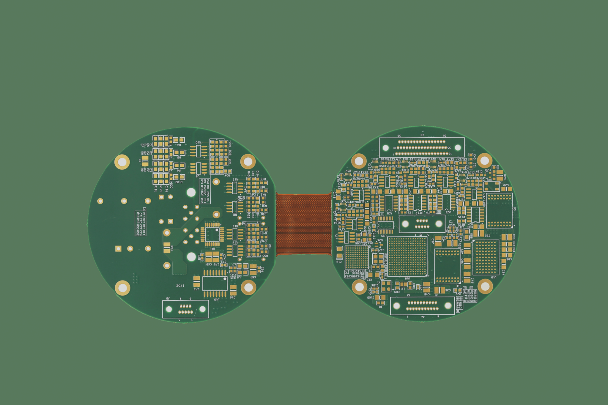
Shape Processing
The shape of single-sided and double-sided printed boards is typically formed through die punching, with upper and lower blanking dies based on board size.
Composite Processing
To enhance productivity, a composite mold can process holes and shapes simultaneously, requiring high precision in design and installation.
Latest Developments
Currently, most PCB manufacturers outsource mold processing to foreign factories to ensure high quality and precision.
Precautions for mold installation include selecting the correct punch, checking machine parts, and maintaining proper alignment to prevent defects.
Improving substrate punching performance can be achieved through preheating paper substrates to 70-90°C.
Quality Defects and Analysis
Common defects include raised hole surroundings, copper foil warping, and misaligned holes. Analysis involves checking punch force, mold design, and machining accuracy.
Factors such as substrate thickness, bonding force, and preheating humidity affect punching quality and should be considered during analysis.