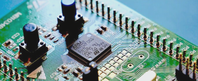
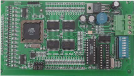
The Importance of PCB Layering in Electronic Design
- PCB boards in modern electronic devices often consist of multiple layers for wiring, including interlayer copper foils for specialized processing.
- Understanding concepts like “multi-layer pad” and “wiring layer setting” is crucial for successful PCB design.
- Properly defining pad characteristics and turning off unused layers can simplify the design process and prevent complications.
Utilizing Vias for Layer Connection
- Via holes are essential for connecting lines between different layers of a PCB.
- Considerations like minimizing via usage and selecting appropriate via sizes based on current carrying capacity are important in circuit design.
Enhancing PCB Functionality with Silkscreen Layers
- Silkscreen layers, or overlays, provide vital information such as component labels, manufacturer logos, and production dates on the PCB surface.
- Proper silkscreen layout is key to ensuring clear markings and preventing issues during assembly and maintenance.
Optimizing SMD Packages and Pad Design
- Special considerations are needed for SMD packages with single-sided element pin holes in PCB design software.
- Customizing pad shapes and sizes based on component requirements is essential for effective PCB layout.
Differentiating Between Grid-like Filling Areas and Pads
- Network filling areas and filling areas serve distinct purposes in circuit design, with network filling areas suppressing interference and filling areas suitable for smaller areas.
- Choosing the right type of pad and filling area can optimize the performance of the PCB.
Understanding the Role of Solder Flux and Solder Mask Films
- Solder flux film improves solderability on pads, while solder mask prevents unwanted tin adhesion during soldering.
- Adjusting settings like “solder Mask Enlargement” ensures proper soldering conditions and component functionality.
Enhancing Routing Efficiency with Flying Lines
- Flying lines aid in observing automatic routing processes and optimizing component positions for efficient routing.
- They can also assist in identifying networks that require manual adjustments during production for optimal performance.