### Basic Knowledge of PCB Design
A **Printed Circuit Board (PCB)** is a fundamental component found in almost every electronic device. Whenever electronic components are present in a device, they are typically mounted on PCBs of various sizes. While the primary function of a PCB is to provide electrical connections between the components, it also serves as a base to mechanically secure and organize the parts. As electronic devices evolve and become more complex, the density of components and circuitry on PCBs continues to increase.
#### Introduction to PCB Design for Beginners
A **bare board** (i.e., a PCB without any components) is often referred to as a **Printed Wiring Board (PWB)**. The board’s substrate is typically made from materials that offer electrical insulation, heat resistance, and mechanical strength. The surface of the board is coated with **copper foil**, which is initially spread across the entire board. During the manufacturing process, portions of the copper are removed through etching, leaving behind a network of conductive traces.
These traces are known as **conductor patterns** or **wiring**, and they provide the electrical pathways that connect various components mounted on the PCB. The components are attached to the PCB by soldering their leads or pins directly onto the conductive traces. In the simplest form of PCB, called a **single-sided PCB**, components are placed on one side of the board, while the copper traces are on the opposite side. To allow electrical connections between both sides, small holes, called **vias**, are drilled through the board, allowing the component pins to pass through and be soldered on the opposite side.
In this configuration, the two sides of the PCB are typically referred to as the **Component Side** (where the components are mounted) and the **Solder Side** (where the soldering takes place). This basic design forms the foundation for more advanced PCB designs, which may involve multi-layer boards, more complex routing, and denser component layouts.
#### Experience-Based Insights for Effective PCB Design
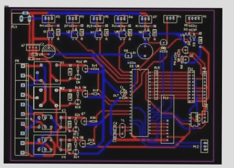
1. **Component Placement and Routing**: As the density of components increases, careful planning of component placement becomes crucial to minimize signal interference and optimize performance. Keep components that are electrically related close to one another to reduce trace lengths and signal degradation.
2. **Trace Width and Spacing**: The width of the copper traces should be selected based on the current they will carry. Overly thin traces may cause overheating or voltage drops, while too-wide traces may increase PCB size unnecessarily. Similarly, the spacing between traces must meet the design rules to avoid short circuits or signal interference.
3. **Via and Hole Design**: Vias are essential for connecting different layers of a PCB, but excessive use of vias can increase manufacturing complexity and cost. Minimizing via usage while ensuring sufficient electrical connectivity is an essential skill for effective PCB design.
4. **Thermal Management**: As electronic components become more powerful, heat dissipation becomes increasingly important. Design considerations such as the use of heat sinks, thermal vias, and the strategic placement of heat-sensitive components are vital to ensuring long-term performance and reliability.
5. **Signal Integrity**: High-speed circuits require careful attention to signal integrity. Factors such as trace impedance, grounding, and minimizing noise should be considered to ensure that signals are transmitted without distortion or interference.
In conclusion, PCB design is a balance of electrical, mechanical, and thermal considerations. The more complex the device, the more intricate the PCB design needs to be. A well-designed PCB ensures not only the efficient operation of the device but also its reliability and durability over time.

### Overview of PCB Components and Technologies
In PCB manufacturing, certain components may need to be removed or reinstalled after production. In such cases, a **socket** (often referred to as a **ZIF** or Zero Insertion Force socket) is used. These sockets are soldered onto the PCB, allowing easy assembly and disassembly of parts, such as CPUs. The ZIF socket is particularly useful as it enables effortless insertion and removal of components without the need for excessive force. A fixing rod next to the socket can secure the part once it’s properly inserted.
### Connecting Multiple PCBs
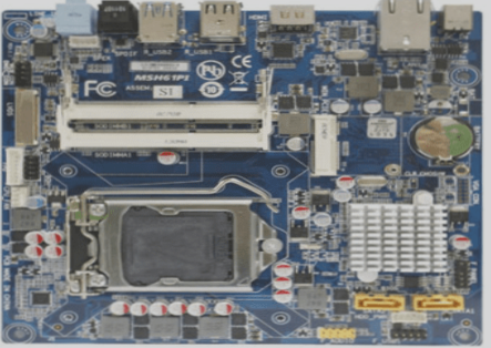
When connecting two PCBs, an **edge connector**, commonly known as a “golden finger,” is typically used. These connectors feature exposed copper pads that are part of the PCB’s wiring. To establish a connection, the golden fingers from one PCB are inserted into a corresponding **expansion slot** on the other. This is a standard method for connecting interface cards, such as display or sound cards, to a motherboard in computers.
The PCB’s **solder mask** layer, often green or brown, acts as an insulating protective cover, shielding the copper traces from damage and preventing incorrect soldering. On top of the solder mask, a **silkscreen** layer is often applied. This layer contains text and symbols (typically white) marking the positions of components on the PCB. This layer is also known as the **legend surface**.
### Types of PCB Designs
1. **Single-Sided Boards**
In a **single-sided** PCB, all components are placed on one side, and the wiring is concentrated on the other side. Since there is only one surface for wiring, the layout is highly constrained. The traces cannot cross each other and must follow a set path around components. Due to these design limitations, single-sided PCBs were predominantly used in early circuit designs.
2. **Double-Sided Boards**
A **double-sided** PCB, as the name suggests, has wiring on both sides of the board. To connect these two sides, a **via** is used—a small hole filled or plated with metal. Vias allow electrical connection between traces on both sides, effectively doubling the available area for routing. This makes double-sided PCBs suitable for more complex circuits than single-sided boards.
3. **Multi-Layer Boards**
Multi-layer PCBs consist of several layers of double-sided boards stacked together, separated by insulating material and bonded under pressure. The number of layers typically ranges from 4 to 8, although advanced designs can feature up to 100 layers, especially in high-performance applications like supercomputers. Multi-layer boards offer substantial routing capacity, allowing for more intricate circuit designs. The layers are generally divided into signal layers, power layers, and ground layers.
In multi-layer PCBs, **blind vias** and **buried vias** are commonly used to create connections between different layers. **Blind vias** connect inner layers to the outer layers without passing through the entire board, while **buried vias** only link internal layers. This approach saves space and reduces the likelihood of wasted space in layers that don’t need to be connected.
### Surface Mount Technology (SMT)
**Surface Mount Technology** (SMT) is widely used in modern PCBs. SMT components have pins that are soldered directly onto the surface of the PCB, eliminating the need for drilling holes as required in through-hole technology (THT). SMT components can be mounted on both sides of the PCB, enabling higher component density compared to traditional THT designs. The compact nature of SMT components allows for smaller and cheaper PCBs, which is why SMT is now the dominant technology in most electronic devices.
However, because SMT components have smaller pins, manual soldering can be difficult, though this is typically not an issue in fully automated assembly lines. Issues with manual soldering are usually encountered during repairs or modifications.
### PCB Design Process
The PCB design process involves several stages:
1. **System Specifications**
Before starting the design, the system requirements must be defined. This includes determining the functionality, cost constraints, size, and operating conditions of the final product.
2. **Manufacturing Process**
The manufacturing process begins with creating the PCB substrate, typically made from glass epoxy or similar materials. The next step involves establishing the circuit layout. This is typically done using a **subtractive transfer** method, where a thin copper foil is applied to the entire surface, and excess material is etched away. Less commonly, an **additive pattern transfer** method is used, which lays copper only where needed.
3. **Assembly Process**
The assembly of SMT components is done using **over reflow soldering**. In this process, solder paste containing flux and solder is applied to the PCB. Components are placed, and the PCB is heated to allow the paste to melt and form solid solder joints. After cooling, the soldering process is complete.
4. **Testing and Quality Control**
After assembly, the PCB undergoes testing to ensure all circuits and components function as expected. Various testing methods, such as electrical tests and functional tests, are performed before the PCB is considered ready for use.
### Cost Considerations
To minimize manufacturing costs, several factors must be taken into account during the design and production process. These include material costs, manufacturing complexity, and the number of layers in the PCB. For instance, using fewer layers or opting for simpler designs can help reduce production costs. Similarly, efficient use of space and the number of components can also impact the overall price.
By understanding and applying these principles, engineers can design and produce efficient, cost-effective PCBs that meet the needs of complex electronic systems.
A **Printed Circuit Board (PCB)** is a fundamental component found in almost every electronic device. Whenever electronic components are present in a device, they are typically mounted on PCBs of various sizes. While the primary function of a PCB is to provide electrical connections between the components, it also serves as a base to mechanically secure and organize the parts. As electronic devices evolve and become more complex, the density of components and circuitry on PCBs continues to increase.
#### Introduction to PCB Design for Beginners
A **bare board** (i.e., a PCB without any components) is often referred to as a **Printed Wiring Board (PWB)**. The board’s substrate is typically made from materials that offer electrical insulation, heat resistance, and mechanical strength. The surface of the board is coated with **copper foil**, which is initially spread across the entire board. During the manufacturing process, portions of the copper are removed through etching, leaving behind a network of conductive traces.
These traces are known as **conductor patterns** or **wiring**, and they provide the electrical pathways that connect various components mounted on the PCB. The components are attached to the PCB by soldering their leads or pins directly onto the conductive traces. In the simplest form of PCB, called a **single-sided PCB**, components are placed on one side of the board, while the copper traces are on the opposite side. To allow electrical connections between both sides, small holes, called **vias**, are drilled through the board, allowing the component pins to pass through and be soldered on the opposite side.
In this configuration, the two sides of the PCB are typically referred to as the **Component Side** (where the components are mounted) and the **Solder Side** (where the soldering takes place). This basic design forms the foundation for more advanced PCB designs, which may involve multi-layer boards, more complex routing, and denser component layouts.
#### Experience-Based Insights for Effective PCB Design
1. **Component Placement and Routing**: As the density of components increases, careful planning of component placement becomes crucial to minimize signal interference and optimize performance. Keep components that are electrically related close to one another to reduce trace lengths and signal degradation.
2. **Trace Width and Spacing**: The width of the copper traces should be selected based on the current they will carry. Overly thin traces may cause overheating or voltage drops, while too-wide traces may increase PCB size unnecessarily. Similarly, the spacing between traces must meet the design rules to avoid short circuits or signal interference.
3. **Via and Hole Design**: Vias are essential for connecting different layers of a PCB, but excessive use of vias can increase manufacturing complexity and cost. Minimizing via usage while ensuring sufficient electrical connectivity is an essential skill for effective PCB design.
4. **Thermal Management**: As electronic components become more powerful, heat dissipation becomes increasingly important. Design considerations such as the use of heat sinks, thermal vias, and the strategic placement of heat-sensitive components are vital to ensuring long-term performance and reliability.
5. **Signal Integrity**: High-speed circuits require careful attention to signal integrity. Factors such as trace impedance, grounding, and minimizing noise should be considered to ensure that signals are transmitted without distortion or interference.
In conclusion, PCB design is a balance of electrical, mechanical, and thermal considerations. The more complex the device, the more intricate the PCB design needs to be. A well-designed PCB ensures not only the efficient operation of the device but also its reliability and durability over time.
### Overview of PCB Components and Technologies
In PCB manufacturing, certain components may need to be removed or reinstalled after production. In such cases, a **socket** (often referred to as a **ZIF** or Zero Insertion Force socket) is used. These sockets are soldered onto the PCB, allowing easy assembly and disassembly of parts, such as CPUs. The ZIF socket is particularly useful as it enables effortless insertion and removal of components without the need for excessive force. A fixing rod next to the socket can secure the part once it’s properly inserted.
### Connecting Multiple PCBs
When connecting two PCBs, an **edge connector**, commonly known as a “golden finger,” is typically used. These connectors feature exposed copper pads that are part of the PCB’s wiring. To establish a connection, the golden fingers from one PCB are inserted into a corresponding **expansion slot** on the other. This is a standard method for connecting interface cards, such as display or sound cards, to a motherboard in computers.
The PCB’s **solder mask** layer, often green or brown, acts as an insulating protective cover, shielding the copper traces from damage and preventing incorrect soldering. On top of the solder mask, a **silkscreen** layer is often applied. This layer contains text and symbols (typically white) marking the positions of components on the PCB. This layer is also known as the **legend surface**.
### Types of PCB Designs
1. **Single-Sided Boards**
In a **single-sided** PCB, all components are placed on one side, and the wiring is concentrated on the other side. Since there is only one surface for wiring, the layout is highly constrained. The traces cannot cross each other and must follow a set path around components. Due to these design limitations, single-sided PCBs were predominantly used in early circuit designs.
2. **Double-Sided Boards**
A **double-sided** PCB, as the name suggests, has wiring on both sides of the board. To connect these two sides, a **via** is used—a small hole filled or plated with metal. Vias allow electrical connection between traces on both sides, effectively doubling the available area for routing. This makes double-sided PCBs suitable for more complex circuits than single-sided boards.
3. **Multi-Layer Boards**
Multi-layer PCBs consist of several layers of double-sided boards stacked together, separated by insulating material and bonded under pressure. The number of layers typically ranges from 4 to 8, although advanced designs can feature up to 100 layers, especially in high-performance applications like supercomputers. Multi-layer boards offer substantial routing capacity, allowing for more intricate circuit designs. The layers are generally divided into signal layers, power layers, and ground layers.
In multi-layer PCBs, **blind vias** and **buried vias** are commonly used to create connections between different layers. **Blind vias** connect inner layers to the outer layers without passing through the entire board, while **buried vias** only link internal layers. This approach saves space and reduces the likelihood of wasted space in layers that don’t need to be connected.
### Surface Mount Technology (SMT)
**Surface Mount Technology** (SMT) is widely used in modern PCBs. SMT components have pins that are soldered directly onto the surface of the PCB, eliminating the need for drilling holes as required in through-hole technology (THT). SMT components can be mounted on both sides of the PCB, enabling higher component density compared to traditional THT designs. The compact nature of SMT components allows for smaller and cheaper PCBs, which is why SMT is now the dominant technology in most electronic devices.
However, because SMT components have smaller pins, manual soldering can be difficult, though this is typically not an issue in fully automated assembly lines. Issues with manual soldering are usually encountered during repairs or modifications.
### PCB Design Process
The PCB design process involves several stages:
1. **System Specifications**
Before starting the design, the system requirements must be defined. This includes determining the functionality, cost constraints, size, and operating conditions of the final product.
2. **Manufacturing Process**
The manufacturing process begins with creating the PCB substrate, typically made from glass epoxy or similar materials. The next step involves establishing the circuit layout. This is typically done using a **subtractive transfer** method, where a thin copper foil is applied to the entire surface, and excess material is etched away. Less commonly, an **additive pattern transfer** method is used, which lays copper only where needed.
3. **Assembly Process**
The assembly of SMT components is done using **over reflow soldering**. In this process, solder paste containing flux and solder is applied to the PCB. Components are placed, and the PCB is heated to allow the paste to melt and form solid solder joints. After cooling, the soldering process is complete.
4. **Testing and Quality Control**
After assembly, the PCB undergoes testing to ensure all circuits and components function as expected. Various testing methods, such as electrical tests and functional tests, are performed before the PCB is considered ready for use.
### Cost Considerations
To minimize manufacturing costs, several factors must be taken into account during the design and production process. These include material costs, manufacturing complexity, and the number of layers in the PCB. For instance, using fewer layers or opting for simpler designs can help reduce production costs. Similarly, efficient use of space and the number of components can also impact the overall price.
By understanding and applying these principles, engineers can design and produce efficient, cost-effective PCBs that meet the needs of complex electronic systems.