PCBA Patch Processing: PCB Hole Plates and Solder Mask Design
In the realm of PCBA patch processing, the intricate design of PCB hole plates and solder masks plays a pivotal role. Let’s explore the processes involved in these two components to gain insight into PCB board and PCBA processing.
Orifice Plate Design in PCB Processing
- The orifice plate design in PCB processing encompasses various types of plates with metallized and non-metallized holes, crucial for the PCB’s processing capacity.
- During PCB production, factors like film and material expansion, material behavior during pressing, and alignment tolerances can lead to pattern misalignments across layers.
- To ensure optimal interconnection, the pad ring width must consider alignment tolerances, insulation gaps, and reliability.
- Metalized hole pad should be ≥ 5 mils.
- Insulation ring width is typically 10 mils.
- Outer layer anti-pad ring width for metallized hole should be ≥ 6 mils, mainly for solder mask requirements.
- Inner layer anti-pad ring width for metallized hole should be ≥ 8 mils, considering insulation gap requirements.
- Anti-pad ring width for non-metallized holes is generally 12 mils.
Solder Mask Design in PCB Processing
- Solder mask gap, bridge width, and cover expansion size depend on solder mask pattern transfer method, surface treatment, and copper thickness.
- Consulting the PCB manufacturer is essential for precise solder mask design.
- With 1 OZ copper thickness, solder mask gap should be ≥ 0.08 mm (3 mils).
- With 1 OZ copper thickness, solder mask bridge width should be ≥ 0.10 mm (4 mils). For lm-Sn surface treatment, a minimum of 0.125 mm (5 mils) bridge width is recommended.
- With 1 OZ copper thickness, minimum expansion size of conductor Tm cover should be ≥ 0.08 mm (3 mils).
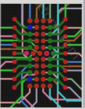
Solder Mask Design for Via Holes in PCBA Processing
- Solder mask design for via holes is critical for manufacturability in PCBA processing, with plug holes dependent on process path and via layout.
- Main methods for solder mask of via holes include plug hole, open small window, and open full window.
- For BGA dog bone connection via hole solder mask, a plug hole design is preferred to minimize bridging and enhance reliability.