Before production begins, you can use an impedance calculator to determine the characteristic impedance of the flexible circuit. The manufacturer of the flexible circuit can assist with this calculation, or you can purchase or download an impedance calculator. Several factors can influence the impedance characteristics of a flexible PCB. The main factors include:
1. The dielectric constant of the insulating material used to construct the circuit
2. The width of the trace carrying the signal
3. The distance between the signal trace and the reference plane layer
4. The thickness of the trace carrying the signal
5. The spacing between signal traces in differential impedance applications
6. Standard double-layer circuit junction
The most common impedance requirements are 50 ohms to 75 ohms (single-ended) or 100 ohms to 110 ohms for differential signals. To achieve these impedance values in a flexible circuit, thicker insulating materials than usual may be required, resulting in a thicker overall circuit.
For double-layer structures with higher impedance requirements, the thickness of the controlled impedance areas is increased, which impacts the flexibility of the circuit.
**Reference Plane and Shielding Layers**
The reference plane layer and the external shielding layer are crucial for impedance control and signal integrity. Manufacturers can add plane layers using the following materials:
– Additional etched copper layer
– Screen-printed conductive epoxy or conductive ink
– Laminated conductive film
For internal planes that need to be connected via plated holes, a copper plane layer is required as the standard reference plane. The copper plane layer helps the flexible circuit maintain its preformed shape, while the screen-printed conductive epoxy, conductive ink, and laminated conductive film enhance the circuit’s flexibility.
**Reinforced Board**

**A wise approach is to use mechanical reinforcement plates to strengthen the SMT components, connectors, and other terminal areas on the flexible circuit.** Flexible circuit manufacturers can incorporate reinforced boards of various thicknesses made from materials like epoxy glass laminate (FR-4) or polyimide film. In SMT applications, a reinforcement board should be placed on the opposite side of the SMT components. In the case of through-hole connectors and other through-hole components, reinforcement plates should be added on the same side as the connectors or through-hole components. When adding a reinforcement board in the connector area, small holes should be provided to match the size of the connector. These small holes in the reinforcement board should be at least 0.015″ larger than the diameter of the clearance hole on the circuit.
**Thermally Isolated Disk**
A thermal isolation pad should be used around each pad surrounded by a large copper area. The extensive copper will dissipate heat from the non-thermally isolated disk, making soldering difficult.
**Rigid-Flex Circuit Design Guide**
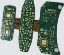
Since the rigid-flex circuit is a hybrid structure combining both rigid and flexible PCBs, specific guidelines apply to this type of design.
**Typical Rigid-Flex Circuit**
On rigid-flex circuits, ensure that all plated through-holes are located in the rigid areas (plated holes should not be in the flexible areas).
Clarify the use of non-adhesive flexible materials and determine whether the rigid-flex design utilizes a “cut-back” covering structure or a “bikini-like” covering structure. Acrylic adhesive is a known weak point for plated holes on rigid-flex circuits. Avoiding the use of acrylic adhesive around plated holes significantly enhances the reliability of these holes.
The rigid areas connected by the flexible circuit should be spaced at least 0.375″ apart, though 0.5″ or more is preferred.
An “unbonded” structure should be used to enhance flexibility. When applying an unbonded structure to a controlled impedance circuit, ensure that the signal and reference plane layers are bonded to each other. When the circuit bends, an unbonded area will flex, which can cause impedance mismatches if the signal and reference layers are not bonded together. After defining the carrier board or “tray” used for component installation, contact the manufacturer to verify that the carrier can properly accommodate their processing panels. Failing to do so could lead to significantly increased costs.
**Factors Affecting Cost**
Designers are always seeking ways to reduce costs without compromising performance. According to IPC research, decisions made by PCB designers influence 75% of circuit costs. It is crucial for flexible circuit designers to understand which features add value and which ones contribute only to higher costs. Designers should never sacrifice reliability to save costs, but at the same time, many features specified for flexible circuits may be unnecessary and only increase costs without providing additional value. The following factors are the primary drivers of increased circuit costs:
**The Number of Circuit Layers:** Increasing the number of layers raises costs by requiring more materials and processing time. Flexible or rigid-flex circuits with many layers can present significant technical challenges, leading to lower yields.
**Circuit Size and Shape:** Flexible circuits are typically cut into puzzle-like shapes. The larger the area the circuit occupies on the panel, the higher the cost. Even slight modifications to the shape of the circuit can result in significant savings. Small adjustments in the circuit’s shape can improve nesting efficiency, potentially allowing for the addition of more circuits per panel.
**Circuit Type (i.e., Category 3 vs. Category 4):** Rigid-flex circuits are generally more expensive than multilayer flexible circuits with reinforced boards. Review your design to determine whether a rigid-flex structure is essential or if a multilayer PCB with a reinforcement board would suffice. If in doubt, consult the flexible PCB manufacturer for guidance.
**Circuit Level (i.e., Level 3 vs. Level 2):** Level 3 circuits require additional testing, inspection, and specific structural requirements, increasing the overall cost. Assess the application requirements to determine which circuit level is necessary.
**Excessive or Strict Dimensional Requirements:** Remember that you are designing a flexible circuit, not a machined part. Flexible circuit materials have looser tolerances than rigid PCB materials, and these tolerances are acceptable. Every dimension added to the design should be verified—ask yourself: “Does this dimension add value or simply increase cost?” Non-critical dimensions should be marked as reference values.
**Consistent Layer Count in Plated Hole Areas:** All areas with plated holes should have the same number of layers and structural integrity.
**Variety of Surface Coatings:** While different surface coatings can be used, this often requires extensive manual masking processes, which can drive up costs.
**Small Features:** Due to the dimensional instability of flexible PCB materials, small features (e.g., via pads) can complicate processing and reduce yield. Evidence shows that using larger features is often more cost-effective than designing with smaller ones.
If your have any questions about PCB ,please contact me info@wellcircuits.com
1. The dielectric constant of the insulating material used to construct the circuit
2. The width of the trace carrying the signal
3. The distance between the signal trace and the reference plane layer
4. The thickness of the trace carrying the signal
5. The spacing between signal traces in differential impedance applications
6. Standard double-layer circuit junction
The most common impedance requirements are 50 ohms to 75 ohms (single-ended) or 100 ohms to 110 ohms for differential signals. To achieve these impedance values in a flexible circuit, thicker insulating materials than usual may be required, resulting in a thicker overall circuit.
For double-layer structures with higher impedance requirements, the thickness of the controlled impedance areas is increased, which impacts the flexibility of the circuit.
**Reference Plane and Shielding Layers**
The reference plane layer and the external shielding layer are crucial for impedance control and signal integrity. Manufacturers can add plane layers using the following materials:
– Additional etched copper layer
– Screen-printed conductive epoxy or conductive ink
– Laminated conductive film
For internal planes that need to be connected via plated holes, a copper plane layer is required as the standard reference plane. The copper plane layer helps the flexible circuit maintain its preformed shape, while the screen-printed conductive epoxy, conductive ink, and laminated conductive film enhance the circuit’s flexibility.
**Reinforced Board**

**A wise approach is to use mechanical reinforcement plates to strengthen the SMT components, connectors, and other terminal areas on the flexible circuit.** Flexible circuit manufacturers can incorporate reinforced boards of various thicknesses made from materials like epoxy glass laminate (FR-4) or polyimide film. In SMT applications, a reinforcement board should be placed on the opposite side of the SMT components. In the case of through-hole connectors and other through-hole components, reinforcement plates should be added on the same side as the connectors or through-hole components. When adding a reinforcement board in the connector area, small holes should be provided to match the size of the connector. These small holes in the reinforcement board should be at least 0.015″ larger than the diameter of the clearance hole on the circuit.
**Thermally Isolated Disk**
A thermal isolation pad should be used around each pad surrounded by a large copper area. The extensive copper will dissipate heat from the non-thermally isolated disk, making soldering difficult.
**Rigid-Flex Circuit Design Guide**
Since the rigid-flex circuit is a hybrid structure combining both rigid and flexible PCBs, specific guidelines apply to this type of design.
**Typical Rigid-Flex Circuit**
On rigid-flex circuits, ensure that all plated through-holes are located in the rigid areas (plated holes should not be in the flexible areas).
Clarify the use of non-adhesive flexible materials and determine whether the rigid-flex design utilizes a “cut-back” covering structure or a “bikini-like” covering structure. Acrylic adhesive is a known weak point for plated holes on rigid-flex circuits. Avoiding the use of acrylic adhesive around plated holes significantly enhances the reliability of these holes.
The rigid areas connected by the flexible circuit should be spaced at least 0.375″ apart, though 0.5″ or more is preferred.
An “unbonded” structure should be used to enhance flexibility. When applying an unbonded structure to a controlled impedance circuit, ensure that the signal and reference plane layers are bonded to each other. When the circuit bends, an unbonded area will flex, which can cause impedance mismatches if the signal and reference layers are not bonded together. After defining the carrier board or “tray” used for component installation, contact the manufacturer to verify that the carrier can properly accommodate their processing panels. Failing to do so could lead to significantly increased costs.
**Factors Affecting Cost**
Designers are always seeking ways to reduce costs without compromising performance. According to IPC research, decisions made by PCB designers influence 75% of circuit costs. It is crucial for flexible circuit designers to understand which features add value and which ones contribute only to higher costs. Designers should never sacrifice reliability to save costs, but at the same time, many features specified for flexible circuits may be unnecessary and only increase costs without providing additional value. The following factors are the primary drivers of increased circuit costs:
**The Number of Circuit Layers:** Increasing the number of layers raises costs by requiring more materials and processing time. Flexible or rigid-flex circuits with many layers can present significant technical challenges, leading to lower yields.
**Circuit Size and Shape:** Flexible circuits are typically cut into puzzle-like shapes. The larger the area the circuit occupies on the panel, the higher the cost. Even slight modifications to the shape of the circuit can result in significant savings. Small adjustments in the circuit’s shape can improve nesting efficiency, potentially allowing for the addition of more circuits per panel.
**Circuit Type (i.e., Category 3 vs. Category 4):** Rigid-flex circuits are generally more expensive than multilayer flexible circuits with reinforced boards. Review your design to determine whether a rigid-flex structure is essential or if a multilayer PCB with a reinforcement board would suffice. If in doubt, consult the flexible PCB manufacturer for guidance.
**Circuit Level (i.e., Level 3 vs. Level 2):** Level 3 circuits require additional testing, inspection, and specific structural requirements, increasing the overall cost. Assess the application requirements to determine which circuit level is necessary.
**Excessive or Strict Dimensional Requirements:** Remember that you are designing a flexible circuit, not a machined part. Flexible circuit materials have looser tolerances than rigid PCB materials, and these tolerances are acceptable. Every dimension added to the design should be verified—ask yourself: “Does this dimension add value or simply increase cost?” Non-critical dimensions should be marked as reference values.
**Consistent Layer Count in Plated Hole Areas:** All areas with plated holes should have the same number of layers and structural integrity.
**Variety of Surface Coatings:** While different surface coatings can be used, this often requires extensive manual masking processes, which can drive up costs.
**Small Features:** Due to the dimensional instability of flexible PCB materials, small features (e.g., via pads) can complicate processing and reduce yield. Evidence shows that using larger features is often more cost-effective than designing with smaller ones.
If your have any questions about PCB ,please contact me info@wellcircuits.com


