1. In daily PCBA processing, the full term for BGA is Ball Grid Array (solder ball array package), which involves arranging solder balls on the underside of the package substrate to serve as the I/O interface for connecting with the printed circuit board (PCB).
2. The devices utilizing this technology are classified as surface mount devices. This packaging method involves an integrated circuit using an organic carrier board.
3. To effectively determine and control the quality of this process, it’s essential to understand and evaluate the physical factors that influence long-term reliability, including solder volume, wire and pad alignment, and wettability.
4. The performance and assembly of BGA devices surpass that of conventional components; however, many manufacturers hesitate to invest in developing mass production capabilities for BGA devices.
5. The primary challenge lies in the difficulty of testing the solder joints of BGA devices, making it hard to ensure their quality and reliability.
In the current information age, the rapid growth of the electronics industry has led to the widespread popularity of products like computers and mobile phones. Consumers now demand more functions and higher performance from electronic devices, while also seeking smaller sizes and lighter weights. This trend has driven the development of electronic products toward multifunctionality, security, miniaturization, and reduced weight. To meet these demands, the feature size of IC chips is continuously decreasing, leading to increased complexity. Consequently, the number of I/Os in circuits is rising, resulting in higher I/O density within packages. To support this advancement, several high-density packaging technologies have emerged, with BGA packaging technology being one of the key players.
Introduced in the early 1990s, BGA packaging has evolved into a mature high-density packaging technology. It experienced the fastest growth among semiconductor IC packaging types from 1996 to 2001, with BGA output reaching around 1 billion in 1999. To date, this technology is best suited for high-density device packaging, and ongoing advancements aim to enhance fine pitch and increase I/O terminal counts. BGA packaging is primarily used for various devices, including PC chipsets, microprocessors/controllers, ASICs, gate arrays, memories, DSPs, PDAs, and PLDs.
Key features of BGA packages in PCBA processing include:
1. Reduced packaging area;
2. Increased functionality and pin count;
3. Self-centering PCB during melting and soldering, facilitating tinning;
4. High reliability, excellent electrical performance, and low overall cost.
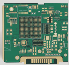
PCBAs processed with BGA typically feature numerous small holes. Most customers design BGA vias with a finished hole diameter of 8-12 mils. For example, the distance between the BGA surface and the hole is 31.5 mils, generally not falling below 10.5 mils. BGA via holes must be plugged, and BGA pads should not be filled with ink or drilled.
In PCBA processing, BGA devices can consistently achieve a defect rate of less than 20 PPM when utilizing standard SMT processes and equipment for assembly. Since the early 1990s, SMT technology has matured; however, the rapid evolution of electronic products toward convenience, miniaturization, networking, and multimedia has raised the bar for electronic assembly technology. As a result, high-density assembly technologies continue to emerge, with BGA (Ball Grid Array package) becoming a prominent solution in practical applications.

