In electronic products and equipment, the PCB is an essential component, playing a crucial role in both the electrical and mechanical connections of the circuit system. Organizing and combining the components on the PCB according to specific requirements is one of the key tasks in PCB design. Layout design goes beyond merely arranging components on the PCB or connecting circuits. Experience has shown that a successful circuit design requires a well-thought-out layout of components, ensuring that the circuit system operates stably and reliably once physically assembled.
On the other hand, an improper component layout can negatively impact PCB performance, potentially causing it to malfunction. This is especially true today with the widespread use of integrated devices. If integrated circuits are mounted using traditional wiring boards, the circuit becomes bulky and may fail to operate stably. Therefore, during product design, both layout and circuit design hold equal importance.
Below is a brief overview of key considerations for RF PCB design:
1. Layout Considerations
(1) Structural Design Requirements
The product’s structure must be defined before starting the PCB layout. The structure needs to be reflected on the PCB, particularly in the areas where the PCB interacts with the structural components (such as the location and shape of the cavity shell). For instance, the outer cavity wall thickness, the inner cavity width, the chamfer radius, and the screw size used for the cavity (e.g., M2, M2.5, M3, M4) should be considered. Specifically, the structural design is based on the outline (or structural parts) drawn on the finished PCB, and the layout is then customized accordingly (if the structure has already been molded in large quantities, this process may differ).
Typically, the outer cavity thickness is 4mm, the inner cavity width is 3mm (or 2mm for the dispensing process), and the chamfer radius is 2.5mm. When designing the PCB, the compartment’s position, starting from the lower left corner of the PCB, must be an integer multiple of 0.5 grid points, with each grid point at least an integer multiple of 0.1. This helps in structural processing and ensures more accurate error control. Of course, these guidelines should be adjusted depending on the specific product type.

(2) **Layout Requirements**
Prioritize the layout of the RF link, followed by the layout of other circuits.
1. The layout of the RF link should follow the sequence defined in the schematic (from input to output, including the sequence of each component and the spacing between them). The distance between certain components should not be too large, such as in a π network. The layout should follow a “straight line” or “L” shape.
In actual RF link layouts, due to space constraints, achieving a “straight line” layout may not always be possible, which often leads to a “U”-shaped layout. A U-shaped layout is not problematic, but it is necessary to introduce a compartment in the middle to isolate and shield the sections on either side. While the reason for this isolation need not be elaborated here, it is important to note that this shield is essential.
In addition, lateral compartments should be considered. Specifically, components arranged in a straight line should be isolated from the left and right by a compartment. This is crucial when dealing with components that are highly sensitive or prone to interference from other circuits. Furthermore, the gain from the input to output of the circuit might be too high, necessitating separation via a cavity.
2. **Peripheral Circuit Layout for Chips**
The layout of peripheral circuits for radio frequency devices must strictly adhere to the specifications in the datasheet, though adjustments can be made depending on space limitations (the components should be placed as close to the chip as possible, provided process requirements are met). The peripheral layout of digital chips is beyond the scope of this discussion.
If the structure includes a metal bottom plate, avoid placing components on the contact surface between the PCB and the bottom plate, and refrain from creating slots in the metal bottom plate.
3. **Wiring Precautions**
Routing should follow the 50-ohm impedance line width, which is typically used as a reference for interlayer connections. The traces should ideally start at the center of the pad, follow straight paths, and be kept on the surface layer where possible. For changes in direction, employ 45-degree angles or arcs. It is advisable to use the pads on both sides of capacitors or resistors as inflection points. If device wiring matching is specified, ensure that the length and shape of the traces follow the datasheet guidelines—for example, the trace length between an amplifier and a capacitor, or the trace length between inductors, should meet the specified requirements.
In PCB design, especially for high-frequency circuits, the following general practices are important to ensure proper design and reduce interference:
(1) **Layer Count**
When designing high-frequency circuit boards, it is advisable to use the inner planes (typically power and ground) as shielding layers. This helps reduce parasitic inductance, minimizes the length of signal traces, and reduces cross-interference between signals.
(2) **Routing Method**
Wires should be routed at 45-degree angles or via circular arcs to reduce signal emissions and mutual coupling, thus minimizing signal reflection.
(3) **Trace Length**
Keep trace lengths as short as possible, and minimize the parallel distance between signal lines.
(4) **Number of Vias**
Minimize the number of vias where possible.
(5) **Layer-to-Layer Routing Direction**
Routing between layers should be perpendicular. For example, if the top layer runs horizontally, the bottom layer should run vertically. This reduces interference between signal traces.
(6) **Copper Coating**
Increase the amount of ground copper to reduce interference between signals.
(7) **Land Pattern**
Encapsulating important signal lines with ground planes significantly enhances the signal’s resistance to interference. Alternatively, interference sources can also be encapsulated to prevent them from affecting other signals.
(8) **Signal Line Routing**
Signal lines should not form loops and must be routed in a daisy-chain manner.
3. **Grounding Treatment**
(1) **Grounding of RF Link**
For the radio frequency section, a multi-point grounding method is typically used. The gap between the copper in the RF link is usually set between 20 mils and 40 mils. Ground holes should be drilled on both sides, with the spacing kept as consistent as possible. Grounding capacitors and resistors in the RF path should have grounding holes placed as close as possible to the components. Similarly, device grounding pads should be connected via holes.
To ensure better contact between the cavity shell and the PCB, two rows of grounding holes are typically punched in a staggered pattern.
The contact area between the PCB and the compartment should be open as a window. Additionally, the section of the ground copper layer on the PCB that interfaces with the bottom plate should also be exposed (but windows should not be used for signal layers) to ensure proper grounding.
For better contact between the PCB, the base, and the cavity shell (improving shielding and heat dissipation), it is important to place screw holes on the PCB.
**Screw Placement for PCB and Cavity Shells**: A screw should be placed at each intersection of the compartment. While achieving this in practice can be challenging, adjustments can be made based on the specific function of the module circuit. However, screws must be placed at the four corners of the cavity shell.
**Screw Placement for PCB and Base**: Each small cavity within the shell should have screws. The number of screws depends on the cavity’s size—the larger the cavity, the more screws are needed. The general rule is to place screws at opposite corners of the cavity. Screws should also be placed near SMA connectors or other types of connectors to prevent deformation of the PCB when connecting or disconnecting components.
On the other hand, an improper component layout can negatively impact PCB performance, potentially causing it to malfunction. This is especially true today with the widespread use of integrated devices. If integrated circuits are mounted using traditional wiring boards, the circuit becomes bulky and may fail to operate stably. Therefore, during product design, both layout and circuit design hold equal importance.
Below is a brief overview of key considerations for RF PCB design:
1. Layout Considerations
(1) Structural Design Requirements
The product’s structure must be defined before starting the PCB layout. The structure needs to be reflected on the PCB, particularly in the areas where the PCB interacts with the structural components (such as the location and shape of the cavity shell). For instance, the outer cavity wall thickness, the inner cavity width, the chamfer radius, and the screw size used for the cavity (e.g., M2, M2.5, M3, M4) should be considered. Specifically, the structural design is based on the outline (or structural parts) drawn on the finished PCB, and the layout is then customized accordingly (if the structure has already been molded in large quantities, this process may differ).
Typically, the outer cavity thickness is 4mm, the inner cavity width is 3mm (or 2mm for the dispensing process), and the chamfer radius is 2.5mm. When designing the PCB, the compartment’s position, starting from the lower left corner of the PCB, must be an integer multiple of 0.5 grid points, with each grid point at least an integer multiple of 0.1. This helps in structural processing and ensures more accurate error control. Of course, these guidelines should be adjusted depending on the specific product type.
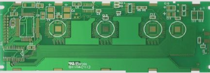
(2) **Layout Requirements**
Prioritize the layout of the RF link, followed by the layout of other circuits.
1. The layout of the RF link should follow the sequence defined in the schematic (from input to output, including the sequence of each component and the spacing between them). The distance between certain components should not be too large, such as in a π network. The layout should follow a “straight line” or “L” shape.
In actual RF link layouts, due to space constraints, achieving a “straight line” layout may not always be possible, which often leads to a “U”-shaped layout. A U-shaped layout is not problematic, but it is necessary to introduce a compartment in the middle to isolate and shield the sections on either side. While the reason for this isolation need not be elaborated here, it is important to note that this shield is essential.
In addition, lateral compartments should be considered. Specifically, components arranged in a straight line should be isolated from the left and right by a compartment. This is crucial when dealing with components that are highly sensitive or prone to interference from other circuits. Furthermore, the gain from the input to output of the circuit might be too high, necessitating separation via a cavity.
2. **Peripheral Circuit Layout for Chips**
The layout of peripheral circuits for radio frequency devices must strictly adhere to the specifications in the datasheet, though adjustments can be made depending on space limitations (the components should be placed as close to the chip as possible, provided process requirements are met). The peripheral layout of digital chips is beyond the scope of this discussion.
If the structure includes a metal bottom plate, avoid placing components on the contact surface between the PCB and the bottom plate, and refrain from creating slots in the metal bottom plate.
3. **Wiring Precautions**
Routing should follow the 50-ohm impedance line width, which is typically used as a reference for interlayer connections. The traces should ideally start at the center of the pad, follow straight paths, and be kept on the surface layer where possible. For changes in direction, employ 45-degree angles or arcs. It is advisable to use the pads on both sides of capacitors or resistors as inflection points. If device wiring matching is specified, ensure that the length and shape of the traces follow the datasheet guidelines—for example, the trace length between an amplifier and a capacitor, or the trace length between inductors, should meet the specified requirements.
In PCB design, especially for high-frequency circuits, the following general practices are important to ensure proper design and reduce interference:
(1) **Layer Count**
When designing high-frequency circuit boards, it is advisable to use the inner planes (typically power and ground) as shielding layers. This helps reduce parasitic inductance, minimizes the length of signal traces, and reduces cross-interference between signals.
(2) **Routing Method**
Wires should be routed at 45-degree angles or via circular arcs to reduce signal emissions and mutual coupling, thus minimizing signal reflection.
(3) **Trace Length**
Keep trace lengths as short as possible, and minimize the parallel distance between signal lines.
(4) **Number of Vias**
Minimize the number of vias where possible.
(5) **Layer-to-Layer Routing Direction**
Routing between layers should be perpendicular. For example, if the top layer runs horizontally, the bottom layer should run vertically. This reduces interference between signal traces.
(6) **Copper Coating**
Increase the amount of ground copper to reduce interference between signals.
(7) **Land Pattern**
Encapsulating important signal lines with ground planes significantly enhances the signal’s resistance to interference. Alternatively, interference sources can also be encapsulated to prevent them from affecting other signals.
(8) **Signal Line Routing**
Signal lines should not form loops and must be routed in a daisy-chain manner.
3. **Grounding Treatment**
(1) **Grounding of RF Link**
For the radio frequency section, a multi-point grounding method is typically used. The gap between the copper in the RF link is usually set between 20 mils and 40 mils. Ground holes should be drilled on both sides, with the spacing kept as consistent as possible. Grounding capacitors and resistors in the RF path should have grounding holes placed as close as possible to the components. Similarly, device grounding pads should be connected via holes.
To ensure better contact between the cavity shell and the PCB, two rows of grounding holes are typically punched in a staggered pattern.
The contact area between the PCB and the compartment should be open as a window. Additionally, the section of the ground copper layer on the PCB that interfaces with the bottom plate should also be exposed (but windows should not be used for signal layers) to ensure proper grounding.
For better contact between the PCB, the base, and the cavity shell (improving shielding and heat dissipation), it is important to place screw holes on the PCB.
**Screw Placement for PCB and Cavity Shells**: A screw should be placed at each intersection of the compartment. While achieving this in practice can be challenging, adjustments can be made based on the specific function of the module circuit. However, screws must be placed at the four corners of the cavity shell.
**Screw Placement for PCB and Base**: Each small cavity within the shell should have screws. The number of screws depends on the cavity’s size—the larger the cavity, the more screws are needed. The general rule is to place screws at opposite corners of the cavity. Screws should also be placed near SMA connectors or other types of connectors to prevent deformation of the PCB when connecting or disconnecting components.

