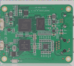
Green Paint Construction Techniques for PCBs
The ball-planting pad beneath a BGA is crucial for successful wave soldering. Using the “green paint set limit” method, it is essential to ensure the green paint thickness does not exceed 1 mil to prevent the “crater effect.” Excess flux and high heat during ball planting can cause solder to seep beneath the green paint, leading to potential lifting issues.
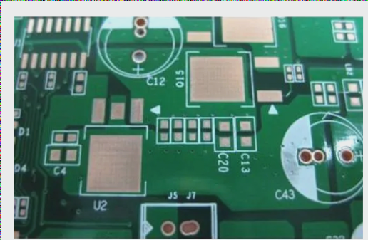
Green Paint Plug Hole Functionality
The green paint plug hole serves to remove empty space for quick fixes during circuit testing and protects nearby circuits from Yong Tin disruption during wave soldering. However, insecure plugs can result in persistent issues due to tin dross pressure. Various construction methods, such as dry film covering and printing flooded holes, aim to achieve perfection but can be challenging.
Reapplying Wave Soldering and BGA Placement
Reapplying wave soldering after fusion welding is common for additional soldering needs, but precautions must be taken to avoid accidental cold welds or open circuits. BGA placement requires precise solder paste printing techniques to prevent disturbances and ensure proper adhesion before welding.
- Steel plate thickness and opening size considerations for different BGA pitches
- Aspect ratio maintenance for paste application
- Rounded corners for square pads to reduce tin particle adhesion
- Optimal particle sizes for solder paste based on BGA type
Challenges and Solutions in PCB Green Paint Construction
Despite advancements in construction techniques, challenges persist in achieving perfection in green paint application and plug hole functionality. Proper understanding and implementation of these methods are crucial to ensuring the reliability and durability of PCBs, especially in the context of lead-free soldering.
Hot Air Fusion Welding in PCB Manufacturing
In the 1990s, hot air fusion welding emerged as the primary method of reflow in PCB manufacturing. With an increased number of heating sections in the production line, adjustments to the “temperature-time curve” have become easier, leading to accelerated production speed. Modern lead-free solderers now come equipped with over 10 heating segments, some even featuring up to 14.
Potential Risks and Considerations
- Prolonged exposure to high temperatures beyond the glass transition temperature (Tg) of the plate can result in the softening of the PCB and lead to Z expansion, potentially causing board failure due to inner circuit or plated through-hole (PTH) fractures.
- The flux in solder paste must reach temperatures above 130°C to activate and should maintain activity for a duration of 90-120 seconds.
- Components have an average heat resistance limit of 220°C, which should not be exceeded for more than 60 seconds to prevent damage.