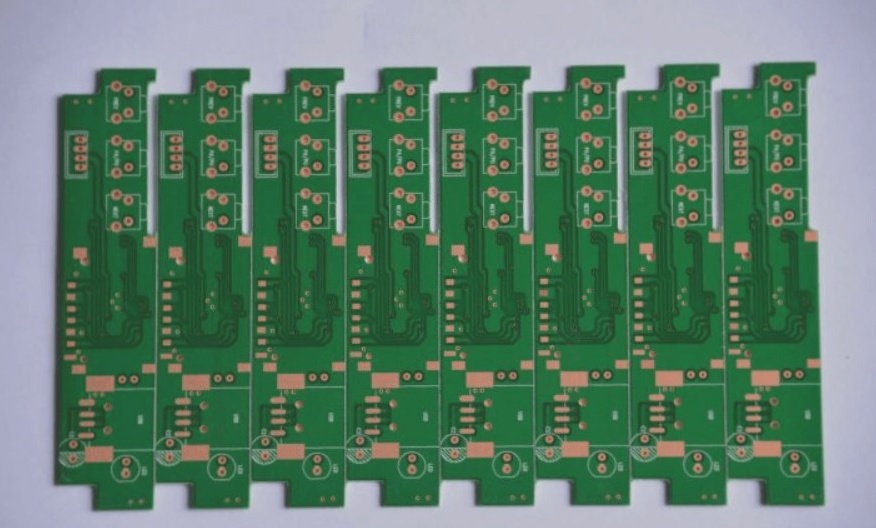
1. Importance of PCB Current Capacity:
- PCB design hinges on understanding current capacity, influenced by factors like wire width, thickness, temperature, and solder resistance.
2. PCB Trace Width and Thickness:
- PCB trace width is the horizontal size of the copper conductor, while thickness is the vertical size.
- Proper calibration minimizes heat buildup, with wider widths lowering resistance and reducing heat accumulation.
3. Factors in Determining Trace Width:
- Considerations include copper layer thickness, cross-sectional area, and trace position (bottom, top, or inner layer).
- Default route width is insufficient; trace width should align with the current carrying capacity.
4. Designing for High Current PCB:
- Different circuits demand varying current capacities; high-power applications may require thicker copper conductors and increased trace width.
- Layout criteria involve reducing wire length to minimize resistance and calculating trace width based on temperature rise and fall.
5. High Current PCB Layout Strategies:
- Isolate sensitive components from high-temperature areas.
- Remove solder resistance to enhance current flow capacity.
- Utilize inner layers for high current routing and copper strips for higher current.
- Apply through-hole stitching to carry multiple wires across layers.
6. Conclusion:
- Designers can rely on thread-thickness calculators for efficient PCB design, emphasizing the importance of correct wiring width and current carrying capacity for reliability and high performance.


