Enhancing PCB Wiring Design for High-Speed Circuits
Printed circuit board (PCB) wiring is a critical aspect of high-speed circuit design, with the schematic serving as its foundation. While a well-crafted schematic is essential, it alone cannot guarantee flawless wiring. Thoughtful schematic drawing is key, emphasizing signal flow throughout the entire circuit.
Key Elements for Comprehensive Schematics:
- Waveform diagrams
- Mechanical casing details
- Printed line lengths
- Component placement on the PCB
- Adjustment guidelines
- Component value ranges
- Heat dissipation specifics
- Controlled impedance for printed lines
- Comments and circuit description summary
It is crucial to provide detailed information in the schematic as circuit designers may not always be available to assist with resolving issues. Additionally, allocating time to review the wiring designer’s work thoroughly is essential for a successful outcome.
Collaboration in Wiring Design Process:
Active involvement in the wiring design process is key to ensuring the PCB meets expectations. Providing guidance and detailed instructions to the wiring engineer can prevent deviations and reduce the need for rework.
Instructions for Wiring Engineer:
- Brief circuit function description
- PCB schematic highlighting input and output positions
- PCB stack-up details
- Signal requirements for each layer
- Critical component placement
- Impedance control requirements
- Length matching needs
- Component sizes and placements
Proper placement of components and meticulous wiring are crucial for achieving design goals, reducing costs, and shortening development cycles. Implementing effective power supply bypassing techniques is essential for noise reduction in high-speed circuits, ensuring optimal performance.
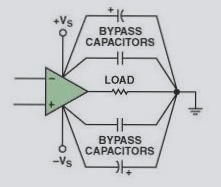
Advantages of Using Multiple Capacitors in Parallel
Figure 1 illustrates the benefits of employing multiple capacitors in parallel on a PCB. Larger capacitors exhibit low impedance at lower frequencies but can become inductive near their resonant frequencies. By utilizing multiple capacitors, a continuous low AC impedance can be maintained across a wide frequency spectrum. This allows for a seamless transition from one capacitor’s resonance to another as the frequency increases. It is crucial to position the capacitors as close as possible to the amplifier, connecting their ground terminals directly to the ground plane through short traces or wires. This connection should be in proximity to the amplifier’s load terminal to minimize interference between power and ground terminals. The process should be repeated for capacitors with progressively larger capacitance values.
Alternative Power Supply Bypassing Method
Alternatively, power supply bypassing can involve one or more capacitors connected across the positive and negative power supply terminals of the operational amplifier. This approach is preferred when configuring four capacitors is impractical but may necessitate larger capacitor sizes due to the increased voltage across them. Despite potential size limitations, this method can enhance Power Supply Rejection (PSR) and reduce distortion in the circuit.
Considerations for Bypass Capacitors
Each circuit and wiring scenario is unique, and the configuration, number, and capacitance of bypass capacitors should align with specific circuit requirements. Parasitic effects, such as capacitance and inductance, can infiltrate PCBs, negatively impacting high-speed circuits. These effects can stem from various sources, including inductive effects from lengthy traces, insufficient ground planes, and capacitive effects from pads to ground or power planes. Even small parasitic values, such as picofarads, can significantly affect circuit performance, leading to frequency response spikes or instability.
Additional Information:
- εr represents the relative permittivity of the PCB board material, while T represents the thickness of the PCB board.
- D1 signifies the diameter of the pad surrounding the through hole, and D2 represents the diameter of the isolation hole in the ground plane, with all dimensions in centimeters.
- A through hole on a 0.157 cm thick PCB board can elevate parasitic inductance to 1.2 nH and parasitic capacitance to 0.5 pF, underscoring the importance of vigilance during PCB wiring to mitigate these parasitic effects.
- The ground plane plays a pivotal role in providing a common reference voltage, offering shielding, heat dissipation, and reducing parasitic inductance, albeit at the expense of increased parasitic capacitance.
- While a ground plane offers numerous benefits, careful implementation is essential due to operational restrictions.
- Optimally, dedicating one PCB layer exclusively as a ground plane is recommended to maintain peak performance, with a strict avoidance of diverting this layer for other signal connections.
- The ground plane’s capacity to suppress magnetic fields between conductors aids in reducing printed line inductance.
- Damage to segments of the ground plane can introduce unexpected parasitic inductance to adjacent printed lines.
- The large surface area and cross-sectional dimensions of the ground plane help maintain its resistance within acceptable limits.
- At lower frequencies, current follows the path of least resistance, while at higher frequencies, it follows the path of least impedance, with exceptions present.
- In specific scenarios, a smaller ground plane may yield superior results, particularly when positioned away from input or output pads to enhance high-speed operational amplifier performance.
- The proximity of the ground plane to input ends can increase the operational amplifier’s input capacitance, reduce phase margin, and induce instability.
- Capacitive loads, inclusive of parasitic capacitances, can introduce poles in feedback loops, further diminishing phase margin and causing circuit instability.
- To minimize interference, it is advisable to isolate analog and digital circuits, along with their respective ground planes, from each other.
- In high-frequency applications, the “skin effect” impacts current flow along the outer surface of wires, elevating DC resistance.
- While not covered in this article, a practical formula can approximate the skin depth in copper wire, aiding in mitigating this effect.
- Wiring and shielding strategies should accommodate various analog and digital signals on the PCB, spanning diverse voltage and current levels from DC to GHz frequencies.
PCB Design Best Practices for Mitigating Interference
- Shortening parallel wire lengths and reducing proximity between signal traces on the same PCB layer can help minimize inductive coupling.
- Minimize long traces on adjacent layers to prevent capacitive coupling, especially for signals requiring high isolation.
- Use controlled impedance printed lines for high-frequency signals, maintaining characteristic impedances like 50Ω.
- Two common types, microstrip lines and strip lines, achieve similar results but differ in implementation methods.
- Dimensions like H (distance from signal trace to ground plane), W (trace width), and T (trace thickness) are crucial, all measured in mils.
- Consider the dielectric constant (εr) of the PCB material when designing controlled impedance lines.
- Strip-shaped controlled impedance printed lines utilize dual ground planes to clamp the signal trace between them.
- Effective PCB layout is critical for successful operational amplifier circuit design, especially in high-speed applications.
- A well-executed schematic is essential for good wiring practices, requiring collaboration between circuit and layout engineers.
- Key considerations include power supply bypassing, minimizing parasitic effects, optimizing ground plane usage, selecting appropriate op-amp packaging, and employing effective PCB wiring and shielding techniques.
- For demanding applications, the strip-shaped controlled impedance printed line method, which requires more PCB layers and is costlier, is typically reserved.