Key Points About PCB Design
-
Line Current Density
In electronic lines, copper on an insulating substrate is common. For circuit boards with 35 μm copper thickness, current density is estimated using the 1A/mm² rule. The line width should be at least 0.3mm for mechanical strength, but non-power boards may have narrower lines. Boards with 70 μm copper thickness are seen in switching power supplies for higher current densities.
-
Design Software Tools
Modern PCB design software includes specifications for line width, spacing, and via hole sizes. These tools automate specifications during design, saving time, reducing workload, and minimizing errors.
-
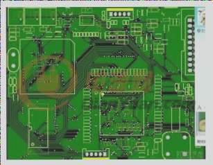
Double-Sided Boards
Double-sided boards are used for high reliability and wiring density. They offer moderate cost and high reliability, suitable for various applications.
-
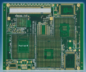
Multi-Layer Boards
Power supply modules use multi-layer boards to integrate components for optimized routing and cooling. These boards offer excellent workmanship and heat dissipation but come with higher costs and reduced flexibility, best for large-scale production.
-
Single-Sided Boards
Universal switching power supplies commonly use single-sided boards due to lower costs. Design and production measures ensure performance despite the cost savings.
-
Single-Sided PCB Design
Single-sided PCBs are widely used in switched power lines for their low cost and ease of manufacture. Careful handling is crucial due to copper being on one side only.


Single-Sided PCB Design Details:
-
To ensure strong bonding, the bonding pad on single-panel PCBs should be slightly larger, preventing peeling or breakage. The pad hole diameter should exceed the pin diameter, with a width over 0.3mm.
-
Electrical connections should be wider than the pad diameter to prevent breakage. In special cases, widening the line (tear drop) when connecting to the pad can avoid issues.
-
Components should be securely attached to the board. Adding sleeves for devices needing heat dissipation can enhance insulation and welding solidity.
-
Lengthening pins on the welded surface can increase strength and aid in quick defect detection. Bending pins before welding can also enhance connection strength.
Double-Panel Design Considerations:
-
Double-sided PCBs excel in high-density environments. Metallized holes offer stronger connections, allowing for smaller rings compared to single panels.
-
Hole diameter on double panels can be slightly larger than pin diameter for improved weld reliability. However, excessively large holes may cause floating parts during soldering.
High-Current Line Design Tips
- Consider tin plating for high-current lines to increase thickness.
- Design routes as bonding pads to ensure tin plating during manufacturing.
- Place pads in wiring, shape as desired, and ensure zero pad hole.
- Provide clear instructions for placing wires in solder-resistant layers.
Tin-Plating Recommendations
- Use long, thin tin-plated strips for wide lines to prevent uneven bonding.
- Utilize double-sided circuit boards for layout flexibility.
- Separate power ground from signal ground and join at filter capacitance.
- Implement point grounding for signal control circuits.
Voltage Feedback and Wiring
- Place feedback voltage sampling point at the power output end for improved load effect index.
- Ensure wiring between layers avoids pin pads to prevent connection damage.
- Recommend at least two holes per 1A current, with a hole size above 0.5mm.
Heat Dissipation in Small Power Sources
- Utilize circuit board wiring for heat dissipation by increasing width.
- Avoid solder on heat dissipation wiring and consider evenly spaced holes for enhanced thermal conductivity.