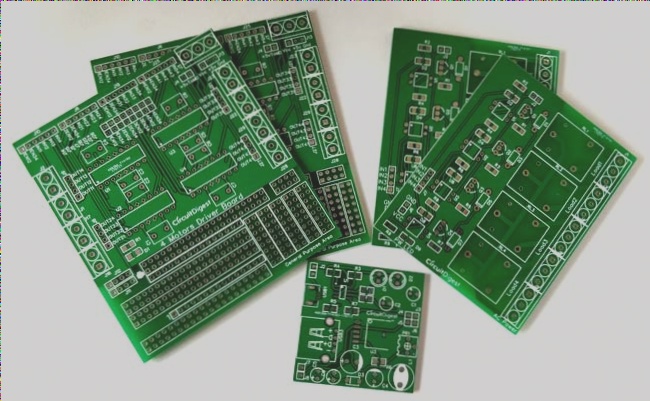
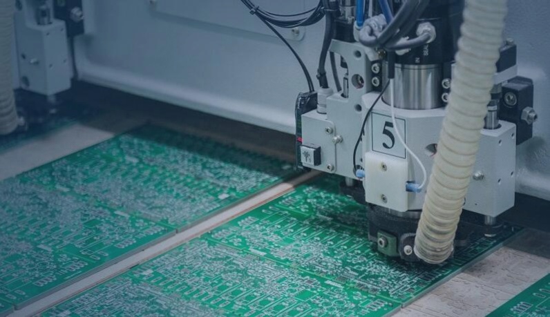
1. In PCB design and layout, adhere to the principle of “big first, then small; difficult first, then easy,” meaning that important unit circuits and core components should be laid out first.
2. Refer to the principle block diagram for the layout, and arrange the main components according to the primary signal flow of the board.
3. Component arrangement should facilitate debugging and maintenance; large components should not be placed around smaller ones or components that require frequent debugging, and there should be ample space around all components.
4. For circuit parts with similar structures, use a “symmetrical” standard layout whenever possible.
5. Optimize the layout according to standards of uniform distribution, balanced center of gravity, and visual appeal.
6. Align plug-in components of the same type in one direction (X or Y). Similarly, polarized discrete components should also be consistently oriented in the X or Y direction to aid in production and inspection.
7. Distribute heating elements evenly to ensure effective heat dissipation across the board and the entire machine. Keep temperature-sensitive devices, other than temperature sensors, away from high-heat-generating components.
8. The layout should aim to meet the following requirements: minimize the total connection length, ensure key signal lines are the shortest; separate high voltage and high current signals from low voltage and low current signals; keep analog signals separate from digital signals; isolate high-frequency signals from low-frequency signals; and ensure adequate spacing for high-frequency components.

It is time for PCB board inspection to focus on some crucial details. To better ensure the quality of the product, the following guidelines should be adhered to when testing the PCB board.
1. **It is strictly forbidden to use grounding test equipment to touch the TV, audio, video, or other equipment on the backplane to detect PCB boards without isolation transformers.** Directly testing TV, audio, video, or other equipment without a power isolation transformer and proper grounding equipment is prohibited. While most recorders have power transformers, special TV or audio equipment with high output power or unknown power supply characteristics require verification. Ensure the chassis is grounded and the equipment is powered off. Short-circuiting TV, audio, or other devices on the backplane due to inadequate power supply isolation can damage integrated circuits and exacerbate failures.
2. **Check the PCB board’s insulation performance of the soldering iron.** Using a soldering iron without confirming it is not electrically charged is not allowed. It is best to ground the soldering iron’s shell. Extra caution is needed for MOS circuits; using a 6~8V low-voltage circuit iron is safer.
3. **Before testing the PCB board, understand the working principles of integrated circuits and related circuits.** Familiarize yourself with the integrated circuit’s function, internal circuit, main electrical parameters, pin functions, normal pin voltages, waveforms, and working conditions. Knowledge of peripheral component principles will simplify analysis and inspection.
4. **Ensure the test PCB board does not cause short circuits between the pins.** When using an oscilloscope probe to measure voltage or test waveforms, avoid short-circuiting IC pins due to probe slippage. It is preferable to measure the peripheral printed circuit directly communicating with the pin. Any short circuit can easily damage the integrated circuit, so exercise extra caution with flat-package CMOS integrated circuits.
5. **Use a PCB tester with high internal resistance.** When measuring DC voltage at IC pins, a multimeter with an internal resistance greater than 20KΩ/V should be used to avoid significant measurement errors in some pin voltages.
6. **Pay attention to the heat dissipation of the power integrated circuit.** Ensure the power integrated circuit has adequate heat dissipation and avoid operating it under high power without a proper heat sink.
7. **Be reasonable when detecting PCB board leads.** If adding external components is necessary, choose small components and ensure reasonable wiring to avoid unnecessary parasitic coupling, especially between the audio power amplifier integrated circuit and the preamplifier circuit.
8. **Ensure the quality of soldering on the PCB board.** During soldering, ensure joints are firm and avoid solder accumulation and porosity. The soldering time should generally be less than 3 seconds, and a soldering iron with around 25W of power is recommended. Carefully inspect the soldered integrated circuit using an ohmmeter to check for short circuits between pins, confirm no solder bridging, and then power on the board.
2. Refer to the principle block diagram for the layout, and arrange the main components according to the primary signal flow of the board.
3. Component arrangement should facilitate debugging and maintenance; large components should not be placed around smaller ones or components that require frequent debugging, and there should be ample space around all components.
4. For circuit parts with similar structures, use a “symmetrical” standard layout whenever possible.
5. Optimize the layout according to standards of uniform distribution, balanced center of gravity, and visual appeal.
6. Align plug-in components of the same type in one direction (X or Y). Similarly, polarized discrete components should also be consistently oriented in the X or Y direction to aid in production and inspection.
7. Distribute heating elements evenly to ensure effective heat dissipation across the board and the entire machine. Keep temperature-sensitive devices, other than temperature sensors, away from high-heat-generating components.
8. The layout should aim to meet the following requirements: minimize the total connection length, ensure key signal lines are the shortest; separate high voltage and high current signals from low voltage and low current signals; keep analog signals separate from digital signals; isolate high-frequency signals from low-frequency signals; and ensure adequate spacing for high-frequency components.

It is time for PCB board inspection to focus on some crucial details. To better ensure the quality of the product, the following guidelines should be adhered to when testing the PCB board.
1. **It is strictly forbidden to use grounding test equipment to touch the TV, audio, video, or other equipment on the backplane to detect PCB boards without isolation transformers.** Directly testing TV, audio, video, or other equipment without a power isolation transformer and proper grounding equipment is prohibited. While most recorders have power transformers, special TV or audio equipment with high output power or unknown power supply characteristics require verification. Ensure the chassis is grounded and the equipment is powered off. Short-circuiting TV, audio, or other devices on the backplane due to inadequate power supply isolation can damage integrated circuits and exacerbate failures.
2. **Check the PCB board’s insulation performance of the soldering iron.** Using a soldering iron without confirming it is not electrically charged is not allowed. It is best to ground the soldering iron’s shell. Extra caution is needed for MOS circuits; using a 6~8V low-voltage circuit iron is safer.
3. **Before testing the PCB board, understand the working principles of integrated circuits and related circuits.** Familiarize yourself with the integrated circuit’s function, internal circuit, main electrical parameters, pin functions, normal pin voltages, waveforms, and working conditions. Knowledge of peripheral component principles will simplify analysis and inspection.
4. **Ensure the test PCB board does not cause short circuits between the pins.** When using an oscilloscope probe to measure voltage or test waveforms, avoid short-circuiting IC pins due to probe slippage. It is preferable to measure the peripheral printed circuit directly communicating with the pin. Any short circuit can easily damage the integrated circuit, so exercise extra caution with flat-package CMOS integrated circuits.
5. **Use a PCB tester with high internal resistance.** When measuring DC voltage at IC pins, a multimeter with an internal resistance greater than 20KΩ/V should be used to avoid significant measurement errors in some pin voltages.
6. **Pay attention to the heat dissipation of the power integrated circuit.** Ensure the power integrated circuit has adequate heat dissipation and avoid operating it under high power without a proper heat sink.
7. **Be reasonable when detecting PCB board leads.** If adding external components is necessary, choose small components and ensure reasonable wiring to avoid unnecessary parasitic coupling, especially between the audio power amplifier integrated circuit and the preamplifier circuit.
8. **Ensure the quality of soldering on the PCB board.** During soldering, ensure joints are firm and avoid solder accumulation and porosity. The soldering time should generally be less than 3 seconds, and a soldering iron with around 25W of power is recommended. Carefully inspect the soldered integrated circuit using an ohmmeter to check for short circuits between pins, confirm no solder bridging, and then power on the board.


