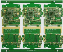
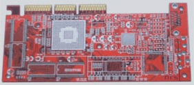
PCB Key Signal Wiring Guidelines
In PCB wiring guidelines, the principle of “key signal line priority” emphasizes prioritizing critical signals like power supply, analog signals, high-speed signals, clock signals, differential signals, and synchronization signals. Let’s delve into the wiring requirements for these key signals:
Analog Signal Wiring Guidelines
- Shorten signal traces to enhance resistance to interference.
- For certain analog signals, impedance control requirements can be relaxed to allow thicker traces.
- Keep analog signals within a designated region separate from digital signals.
High-Speed PCB Signal Wiring Recommendations
- Utilize Multilayer PCBs:
- High-speed circuits benefit from multilayer boards to reduce interference and improve grounding.
- Proper layer selection can minimize signal transmission lengths and cross-interference.
- Minimize Trace Bends:
- Limit bends in high-speed signal traces for optimal performance.
- Optimize Lead Design:
- Use straight leads or 45° angles to reduce emissions and signal coupling.
- Shorter leads improve signal transmission by minimizing inductance and capacitance.
- Reduce vias between pins to enhance circuit speed.
- Avoid parallel traces and stubs to prevent impedance issues.
- Route High-Frequency Signals Internally:
- Route high-frequency signals on inner layers to reduce electromagnetic radiation.

Clock Signal Routing Instructions
The Importance of Clock Signal Routing in PCB Design
In digital circuit design, the clock signal is vital as it oscillates between high and low states, ensuring proper circuit operation. The clock network’s performance significantly impacts circuit functionality and can emit electromagnetic radiation. When laying out a PCB, special attention must be given to routing the clock signal effectively.
- Plan the clock tree early to define relationships between different clocks.
- Considerations for clock signal routing:
- Choose the optimal layer for routing.
- Avoid crossing or routing through split planes.
- Maintain a distance of 3W between clock signals and other traces.
- Use inner layers for longer clock traces in EMC-compliant designs.
- Ensure proper termination matching.
- Implement a star structure for signal distribution.
- Keep traces connected to the crystal oscillator short.
- Optimize ground connections for crystal capacitors.
- Surround clock traces with ground planes to reduce crosstalk.
Differential Signal Routing Requirements
Differential signals involve pairs of signals with opposite polarities transmitting data based on voltage differences. To maintain signal integrity:
- Route the two traces parallel with equal length.
- Maintain consistent width and spacing for the traces.
General Tips for PCB Routing
For critical signals like clock and high-frequency ones, designate specific layers for routing. Minimize loop area, use shielding, and increase clearance for optimal signal integrity.
If you have any PCB questions, feel free to reach out to us at info@wellcircuits.com.