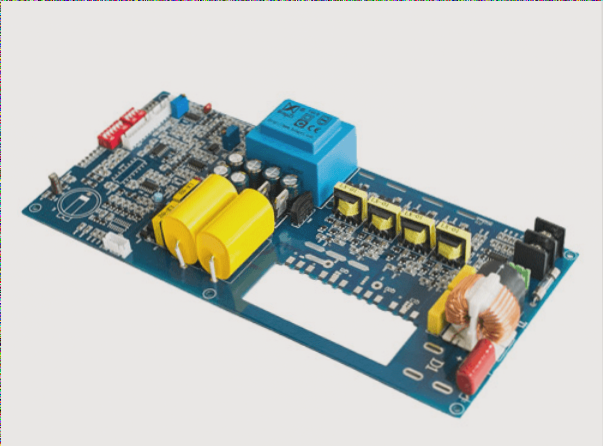
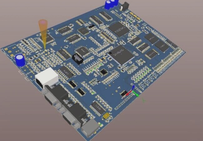
The silk-screen layer is primarily intended for manual assembly and adjustments to the board. It provides information to the operator during the assembly process, such as component placements, reference designators, and other important labels.
The assembly layer, on the other hand, is specifically used to indicate the physical size of components and is primarily used during the automated assembly process. It assists placement machines in correctly positioning and soldering components. This layer can also include component values, such as resistance and capacitance values, which aids in both the assembly and maintenance of the PCB.
In PCB design, we often encounter the terms solder mask and paste mask. Although we may have a general understanding that the solder mask refers to the protective layer and the paste mask pertains to the solder paste area, this distinction becomes more important when creating custom pads in design software like Cadence.
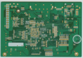
**Solder Mask:** The solder mask is the protective layer, often referred to as the anti-display layer. It is applied to the outer layer of the PCB over pads (including surface-mount pads, through-hole pads, and vias) to prevent unwanted soldering during the PCB’s journey through the soldering furnace (wave soldering). The green layer that is commonly seen on most PCBs is the solder mask, but it can also appear in other colors such as blue or red. The solder mask layer prevents solder from covering areas that do not require it.
The solder mask layer is divided into two parts: Top and Bottom layers. The solder mask exposes the pads, which are typically represented as small circles or squares when the solder mask layer is displayed. This exposure is usually larger than the actual pad area, as the solder mask material needs to cover the surrounding copper traces while leaving the pad exposed for soldering.
When generating Gerber files, you can see the actual effect of the solder mask layer. For example, if you draw a solid rectangle on the solder mask layer (TopSolder or BottomSolder), it essentially creates a window without solder mask (revealing the underlying copper). Solder mask materials, such as green, blue, or red, can be used, but they should not be applied to pads, vias, or any other areas where soldering is needed. Typically, the solder mask is designed to be about 0.15mm (6 mils) larger than the actual pad size when creating custom pads in Cadence.

1. **Paste Mask Layers (Solder Paste Protective Layer)**: This is a positive display; where there is nothing, there is nothing. It is used for surface mount (SMD) components. This layer is designed to create the steel stencil (sheet), and the holes in the stencil align with the solder pads of the SMD devices on the PCB. When soldering surface-mount devices, the steel stencil is first placed on the PCB (aligning with the actual pads), then solder paste is applied. Excess paste is scraped off with a squeegee, and the stencil is removed. This process leaves solder paste on the pads, and the SMD component is then placed onto the paste (either manually or using a pick-and-place machine). Finally, the SMD component is soldered in a reflow soldering oven. The aperture size in the stencil is usually smaller than the pad size on the PCB. By specifying an expansion rule, the paste mask layer can be adjusted to enlarge or reduce the apertures. For different pad requirements, multiple rules can be defined in the paste mask layer. The system also provides two solder paste protection layers: the top solder paste layer (Top Paste) and the bottom solder paste layer (Bottom Paste). A solid rectangle is drawn in the paste mask layers (Top Paste and Bottom Paste), with a window opened inside the rectangle where solder paste is sprayed. Essentially, the stencil creates a window for wave soldering to tin the pads.
2. **Keepout vs. Mechanical Layers**: These two layers are often confused. The keepout layer defines the electrical boundaries by drawing a border, while the mechanical layer represents the actual physical boundary. The positioning holes are created according to the mechanical layer’s dimensions. However, PCB factory engineers might not always fully understand this distinction. Therefore, it’s best to remove the keepout layer before sending the design to the factory (there was a situation in the lab where the keepout layer was not deleted, causing the factory to cut the wrong boundary).
3. **Assembly Layer vs. Silkscreen Layer**: The assembly layer and the silkscreen layer are often encountered in PCB design. So, what do these layers represent?
– **Silkscreen Layer**: This layer shows the outline of the components. It consists of graphic symbols representing the devices’ outlines. During PCB design, this layer’s data is often used for light drawing. More commonly, the silkscreen is printed on the PCB to show component outlines.
– **Assembly Layer**: This layer includes the physical shapes of the parts, marked as “PLACE BOUND TOP/BOTTOM.” It is used for Design for Manufacturing (DFM) and Design for Assembly (DFA) rules. This layer helps layout and assembly checks by indicating where parts should be placed and confirming proper part positioning. It’s useful when verifying whether all components are correctly aligned before assembly. While the silkscreen layer is necessary, the assembly layer is not always required (this is a personal view).
4. **Jiefang Factory and PCB Design Institute**: Recently, Jiefang Factory launched a PCB Design Institute. PCB enthusiasts and designers are welcome to visit the institute’s website. Thank you.
5. **Positive vs. Negative Film in PCB Design**: The terms “positive film” and “negative film” refer to two different methods of displaying a layer’s content. Regardless of whether a positive or negative film is used, the final PCB remains the same. The difference lies in how data is processed in the software, such as during DRC (Design Rule Check) detection or cadence processing. The positive film displays what is physically present—wires, pads, and components are visible. In contrast, negative film shows what is not there—the copper areas that need to be etched. Neither film type is inherently superior to the other. For example, Jiefang Factory uses negative film technology, which offers better circuit accuracy and tolerance control. Since holes are sealed by the negative film, unsealed holes are exposed directly to the etching liquid, ensuring no copper is retained in those areas, making non-metallized holes more reliable. The positive film process is more commonly used in PCB factories, with a longer history and mature processing methods. It is more adaptable to unconventional processes, like semi-hole or edge processes. The advantage of positive film is that if components or vias need re-plating, comprehensive DRC verification can be done. On the other hand, the negative film automatically updates copper without re-laying, without the need for DRC verification.
6. **Through-Hole Pads Design**: When designing through-hole pads, the hole diameter should be 10 mils (0.2 mm) larger than the component pin, and the outer diameter of the pad should be at least 20 mils larger than the hole. If the pad is too small, it becomes difficult to solder properly.
If you have any PCB manufacturing needs, please do not hesitate to contact me.Contact me


