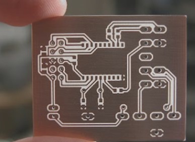
The attached image is part of my pcb from Kicad. If you look at the triangular gnd plane there is a 10K resistor and 0.1uF cap connected on their gnd pins and then there is a via going to the gnd plane. However, that part of the gnd plane is isolated from the rest of the gnd plane and there are lots of other gnd pins.
When I run DRC it says everything is connected, but these gnd pins aren’t actually connected to other gnd pins. If I delete the via then kicad recognizes that area of the pcb shouldn’t be ground filled. However it seems to think if a single gnd pin has a via to the plan then that plan is connected to all gnd pins.
Is is a known issue with Kicad’s drc or is there some setting I should change?
Thanks in advance!


