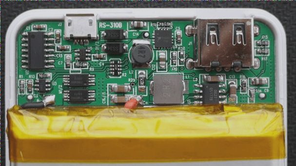
The Latest Trends in HDI PCB Technology
High-density interconnect (HDI) PCBs continue to revolutionize the PCB industry with their superior circuit density and innovative design features. HDI PCBs now support even smaller vias, capture pads, and increased connection pad densities, making them ideal for cutting-edge electronics applications.
With advancements in blind and buried vias, HDI boards now boast micro vias as tiny as 0.006 inches in diameter, enabling unprecedented miniaturization and performance enhancements.
Applications of HDI PCBs
HDI PCBs are the go-to choice for a wide range of devices, including smartphones, tablets, laptops, digital cameras, 5G network equipment, and medical devices. Their compact size and high performance make them indispensable in modern electronics.
Key Benefits of HDI PCB Technology
- Enhanced packaging density for more components
- Simplified routing, especially for dense components
- Improved signal transmission and reduced signal loss
- Minimized crossing delays for faster operation
Enhanced Functions Enabled by HDI PCBs
- Higher trace routing density for complex designs
- Stable power distribution across the board
- Reduced interference from inductance and capacitance
- Enhanced signal integrity for high-speed applications
Boost Your Development Process with HDI PCBs
- Effortless placement of surface mount components
- Speedier routing capabilities
- Less need for component rearrangement
- Expanded component space facilitated by Via-in-Pad technology
For inquiries regarding PCBs or PCBA services, reach out to us at info@wellcircuits.com.


