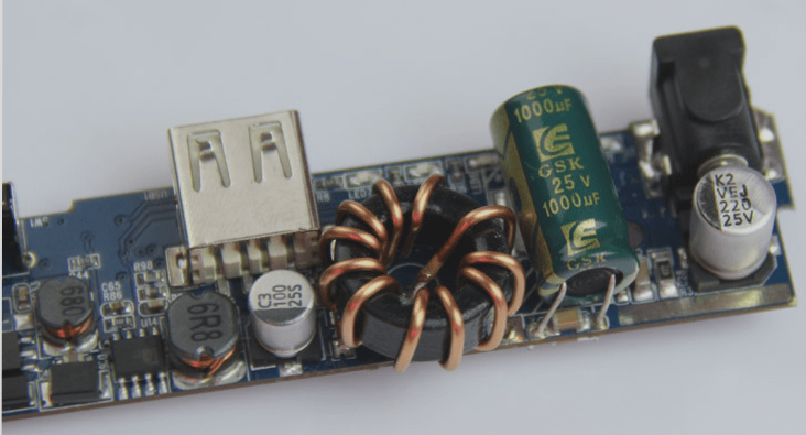
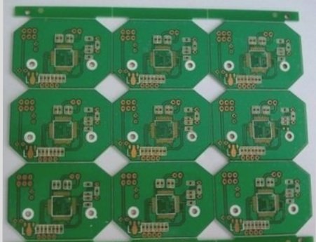
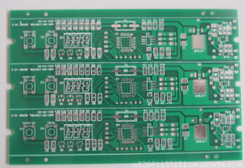
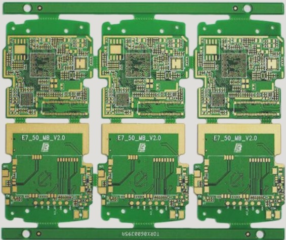
**Introduction to HDI PCB Boards**
HDI (High-Density Interconnector) PCBs are advanced circuit boards designed with high-density wiring and interconnection features. These boards employ micro-blind and buried via technologies to achieve a compact design and efficient signal transmission. Typically, HDI PCBs consist of both inner and outer layer circuits. Through precise processes such as drilling and metallization, these layers are interconnected, facilitating the complex routing of signals. The result is a PCB that supports a higher degree of miniaturization, improved performance, and greater functionality, making it ideal for applications in industries like telecommunications, automotive, and consumer electronics.
HDI technology enhances traditional PCB designs by allowing for smaller via sizes and higher wiring density. This leads to improved electrical performance and reduced size, which is essential in today’s increasingly miniaturized electronic devices.

HDI (High-Density Interconnect) boards are typically manufactured using a layer-by-layer process. As the number of layers increases, the technical complexity and grade of the board also rise. Basic HDI boards are often created through a one-time build-up method. In contrast, high-end HDI boards utilize multiple build-up stages, incorporating advanced PCB technologies such as stacking holes, electroplating, hole filling, and laser direct drilling. These techniques enhance both the board’s functionality and performance.
When the PCB density exceeds that of an eight-layer board, HDI technology is typically employed. HDI boards are more cost-effective than traditional, complex lamination processes, offering a significant advantage in terms of both cost and performance. These boards support advanced packaging technologies, and their electrical performance, signal integrity, and overall accuracy are superior to conventional PCBs. Additionally, HDI boards are better at mitigating issues related to radio frequency interference (RFI), electromagnetic wave interference (EMI), electrostatic discharge (ESD), and heat conduction.
**Are boards with blind and buried holes considered HDI boards?**
Not all boards with blind or buried holes are classified as HDI boards. HDI boards are specifically designed for high-density interconnects, and these boards may incorporate blind holes that are plated and laminated. HDI boards are categorized into different levels: first-order, second-order, third-order, and fourth-order. Fifth-order HDI boards are not simply defined by the use of buried holes but involve more complex designs and processes.
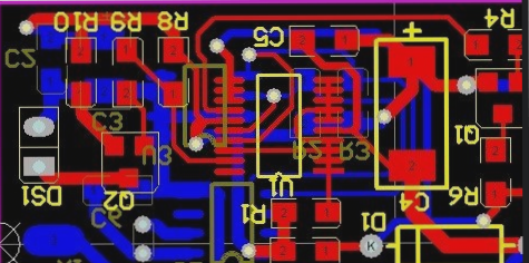
**Distinguishing HDI Board Types**
– **First-order HDI boards** are the simplest and involve a straightforward process that is easy to control. The interconnection between layers is relatively basic, with fewer alignment issues or manufacturing challenges.
– **Second-order HDI boards** are more complex, primarily due to alignment challenges and the need for precise punching and copper plating. There are several variations in second-order designs:
1. Some designs stagger the positions of each layer. To connect adjacent layers, a wire is routed through the middle layer, essentially creating a setup similar to two first-order HDI boards.
2. Other designs overlap the holes of two first-order HDI boards. This superimposition method introduces additional process points that require careful control and precision.
3. Another approach directly punches from the outer layer to the third (or N-2) layer. This process is more challenging than the previous two, as the punching difficulty increases.
– **Third-order HDI boards** are analogous to second-order boards but involve even more intricate manufacturing techniques, such as direct punching through multiple layers, which introduces higher complexity and precision requirements.
**Printed Circuit Board (PCB) Ink**
PCB ink, also known as printed circuit board ink, is a specialized type of ink designed for use in PCB manufacturing. It has unique physical properties, including viscosity, thixotropy, and fineness, which are crucial for achieving optimal printing performance. Understanding these properties can help improve ink application and enhance the overall quality of the printed circuits. Proper control of these ink characteristics ensures the best printing outcomes during PCB production, which contributes to the board’s performance and reliability.
In the process of printed circuit board (PCB) production, achieving high-quality image reproduction relies heavily on the ink’s viscosity and thixotropy. But what exactly are these properties?
**Viscosity** refers to the internal friction within a liquid. It measures the resistance one layer of liquid exerts on another when subjected to an external force. Essentially, it reflects how easily a liquid flows. Temperature plays a crucial role in viscosity—higher temperatures tend to reduce viscosity, making the ink thinner and easier to work with, while lower temperatures increase its resistance. For example, a thick liquid layer encounters greater mechanical resistance when sliding, while a thinner liquid flows more easily.
**Thixotropy**, on the other hand, is a unique characteristic of certain liquids where their viscosity decreases under agitation but returns to its original state once the stirring ceases. This property is particularly important for ensuring consistent screen printing results. During the squeegee process, ink is agitated, becoming more fluid, which helps it pass through the mesh faster and achieve a more uniform distribution. Once the squeegee stops, the ink regains its initial viscosity, ensuring the print quality remains intact. Manual operations require skilled technicians to maintain uniformity throughout the process, while mechanical operations are simpler and more consistent.
Another key aspect of ink quality is its **fineness**. The pigments and mineral fillers in the ink are typically solid and should be finely ground to particles no larger than 4 to 5 microns. This precise particle size creates a homogeneous fluid state, which ensures that the printed solder mask has a consistent, full, and uniform appearance.
### Key Considerations for Ink Use:
1. **Temperature Control**: The ink should always be maintained at temperatures between 20-25°C. Significant temperature fluctuations can affect the viscosity and, consequently, the screen printing quality. When storing ink in environments with varying temperatures, it’s essential to allow it to adjust to the proper ambient temperature before use. Using cold ink can lead to printing failures and other issues, so maintaining a stable temperature is critical for optimal performance.
2. **Proper Mixing**: Before use, ink must be thoroughly mixed, either manually or mechanically. Air trapped in the ink can affect its performance, so it should be allowed to stand for a while if bubbles are present. If the ink needs dilution, it should be mixed thoroughly and its viscosity checked. After use, the ink container should be sealed tightly, and any leftover ink on the screen should never be returned to the ink tank.
3. **Cleaning and Maintenance**: A dedicated cleaning agent should be used to clean ink residue from equipment. This cleaning process must be thorough to ensure no contamination between different ink colors. It’s best to use a clean solvent to avoid any impact on the quality of subsequent ink applications.
4. **Drying Process**: Once printed, the ink must be dried in a well-ventilated area with a good exhaust system. This ensures that the ink retains its quality and doesn’t undergo any undesirable changes.
In summary, achieving high-quality PCB screen printing requires careful attention to ink properties like viscosity and thixotropy, along with strict adherence to temperature control, proper mixing, thorough cleaning, and efficient drying procedures. Maintaining the correct operating conditions and following these guidelines ensures consistent results and avoids unnecessary production issues.
HDI (High-Density Interconnector) PCBs are advanced circuit boards designed with high-density wiring and interconnection features. These boards employ micro-blind and buried via technologies to achieve a compact design and efficient signal transmission. Typically, HDI PCBs consist of both inner and outer layer circuits. Through precise processes such as drilling and metallization, these layers are interconnected, facilitating the complex routing of signals. The result is a PCB that supports a higher degree of miniaturization, improved performance, and greater functionality, making it ideal for applications in industries like telecommunications, automotive, and consumer electronics.
HDI technology enhances traditional PCB designs by allowing for smaller via sizes and higher wiring density. This leads to improved electrical performance and reduced size, which is essential in today’s increasingly miniaturized electronic devices.
HDI (High-Density Interconnect) boards are typically manufactured using a layer-by-layer process. As the number of layers increases, the technical complexity and grade of the board also rise. Basic HDI boards are often created through a one-time build-up method. In contrast, high-end HDI boards utilize multiple build-up stages, incorporating advanced PCB technologies such as stacking holes, electroplating, hole filling, and laser direct drilling. These techniques enhance both the board’s functionality and performance.
When the PCB density exceeds that of an eight-layer board, HDI technology is typically employed. HDI boards are more cost-effective than traditional, complex lamination processes, offering a significant advantage in terms of both cost and performance. These boards support advanced packaging technologies, and their electrical performance, signal integrity, and overall accuracy are superior to conventional PCBs. Additionally, HDI boards are better at mitigating issues related to radio frequency interference (RFI), electromagnetic wave interference (EMI), electrostatic discharge (ESD), and heat conduction.
**Are boards with blind and buried holes considered HDI boards?**
Not all boards with blind or buried holes are classified as HDI boards. HDI boards are specifically designed for high-density interconnects, and these boards may incorporate blind holes that are plated and laminated. HDI boards are categorized into different levels: first-order, second-order, third-order, and fourth-order. Fifth-order HDI boards are not simply defined by the use of buried holes but involve more complex designs and processes.
**Distinguishing HDI Board Types**
– **First-order HDI boards** are the simplest and involve a straightforward process that is easy to control. The interconnection between layers is relatively basic, with fewer alignment issues or manufacturing challenges.
– **Second-order HDI boards** are more complex, primarily due to alignment challenges and the need for precise punching and copper plating. There are several variations in second-order designs:
1. Some designs stagger the positions of each layer. To connect adjacent layers, a wire is routed through the middle layer, essentially creating a setup similar to two first-order HDI boards.
2. Other designs overlap the holes of two first-order HDI boards. This superimposition method introduces additional process points that require careful control and precision.
3. Another approach directly punches from the outer layer to the third (or N-2) layer. This process is more challenging than the previous two, as the punching difficulty increases.
– **Third-order HDI boards** are analogous to second-order boards but involve even more intricate manufacturing techniques, such as direct punching through multiple layers, which introduces higher complexity and precision requirements.
**Printed Circuit Board (PCB) Ink**
PCB ink, also known as printed circuit board ink, is a specialized type of ink designed for use in PCB manufacturing. It has unique physical properties, including viscosity, thixotropy, and fineness, which are crucial for achieving optimal printing performance. Understanding these properties can help improve ink application and enhance the overall quality of the printed circuits. Proper control of these ink characteristics ensures the best printing outcomes during PCB production, which contributes to the board’s performance and reliability.
In the process of printed circuit board (PCB) production, achieving high-quality image reproduction relies heavily on the ink’s viscosity and thixotropy. But what exactly are these properties?
**Viscosity** refers to the internal friction within a liquid. It measures the resistance one layer of liquid exerts on another when subjected to an external force. Essentially, it reflects how easily a liquid flows. Temperature plays a crucial role in viscosity—higher temperatures tend to reduce viscosity, making the ink thinner and easier to work with, while lower temperatures increase its resistance. For example, a thick liquid layer encounters greater mechanical resistance when sliding, while a thinner liquid flows more easily.
**Thixotropy**, on the other hand, is a unique characteristic of certain liquids where their viscosity decreases under agitation but returns to its original state once the stirring ceases. This property is particularly important for ensuring consistent screen printing results. During the squeegee process, ink is agitated, becoming more fluid, which helps it pass through the mesh faster and achieve a more uniform distribution. Once the squeegee stops, the ink regains its initial viscosity, ensuring the print quality remains intact. Manual operations require skilled technicians to maintain uniformity throughout the process, while mechanical operations are simpler and more consistent.
Another key aspect of ink quality is its **fineness**. The pigments and mineral fillers in the ink are typically solid and should be finely ground to particles no larger than 4 to 5 microns. This precise particle size creates a homogeneous fluid state, which ensures that the printed solder mask has a consistent, full, and uniform appearance.
### Key Considerations for Ink Use:
1. **Temperature Control**: The ink should always be maintained at temperatures between 20-25°C. Significant temperature fluctuations can affect the viscosity and, consequently, the screen printing quality. When storing ink in environments with varying temperatures, it’s essential to allow it to adjust to the proper ambient temperature before use. Using cold ink can lead to printing failures and other issues, so maintaining a stable temperature is critical for optimal performance.
2. **Proper Mixing**: Before use, ink must be thoroughly mixed, either manually or mechanically. Air trapped in the ink can affect its performance, so it should be allowed to stand for a while if bubbles are present. If the ink needs dilution, it should be mixed thoroughly and its viscosity checked. After use, the ink container should be sealed tightly, and any leftover ink on the screen should never be returned to the ink tank.
3. **Cleaning and Maintenance**: A dedicated cleaning agent should be used to clean ink residue from equipment. This cleaning process must be thorough to ensure no contamination between different ink colors. It’s best to use a clean solvent to avoid any impact on the quality of subsequent ink applications.
4. **Drying Process**: Once printed, the ink must be dried in a well-ventilated area with a good exhaust system. This ensures that the ink retains its quality and doesn’t undergo any undesirable changes.
In summary, achieving high-quality PCB screen printing requires careful attention to ink properties like viscosity and thixotropy, along with strict adherence to temperature control, proper mixing, thorough cleaning, and efficient drying procedures. Maintaining the correct operating conditions and following these guidelines ensures consistent results and avoids unnecessary production issues.