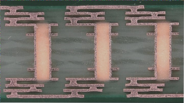
2. **Blind Via Hole:** The outermost circuit of the blind buried via circuit board connects with adjacent inner layers through plating holes, known as “blind vias,” because the opposite side cannot be seen. To increase PCB circuit layer space utilization, the “blind via” process was developed. This production method requires careful attention to the drilling hole depth (Z-axis) to ensure precision, though it often presents challenges with hole electroplating, limiting its adoption by manufacturers.
3. Blind vias are located on the top and bottom surfaces of the printed circuit board, have a specific depth, and are used to connect surface lines with underlying inner layer lines. The depth of these holes typically does not exceed a certain ratio relative to their diameter.
4. In non-penetrating via technology, the application of blind and buried vias can significantly reduce the size and quality of circuit boards with blind and buried holes, decrease layer counts, enhance electromagnetic compatibility, improve electronic product characteristics, reduce costs, and simplify and expedite design work. Traditional PCB design and fabrication face several issues with through-holes.
5. Firstly, they occupy a significant amount of effective space. Secondly, a concentration of numerous through-holes in one area poses a substantial obstacle for the inner layers of multi-layer PCBs. These through-holes occupy space required for traces, densely traverse the power supply and ground layers, and disrupt the impedance characteristics of the power-ground layers, leading to power-ground layer failures. Using conventional mechanical drilling increases workload by up to 20 times compared to non-penetrating pilot hole technology.

HDI stackup
In PCB design, as the size of pads and vias has gradually decreased, the thickness of board layers must decrease proportionally to avoid increasing the aspect ratio of through holes, which reduces reliability. Advanced laser drilling and plasma dry etching technologies now enable the use of non-penetrating small blind and buried holes. For instance, with a 0.3mm diameter, these holes introduce parasitic parameters only about 1/10th of conventional holes, significantly enhancing PCB reliability.
Non-penetrating via technology reduces the number of large vias on the PCB, thereby freeing up more space for traces. This additional space supports large-area shielding, enhancing EMI/RFI performance. Moreover, it provides room for inner layer shielding of critical components and network cables, optimizing electrical performance. Non-penetrating vias also facilitate easier fan-out of device pins, particularly beneficial for routing high-density devices like BGA packages, reducing signal path lengths to meet high-speed circuit timing requirements.
The evolution of HDI PCB technology offers engineers unprecedented design flexibility to densely populate both sides of the PCB with smaller components, enhancing signal transmission speed and quality.
HDI PCBs find extensive use in reducing product weight and size while improving device electrical performance. They are prevalent in mobile phones, touchscreens, laptops, digital cameras, and 4G network communication devices. HDI PCBs also play a crucial role in medical devices and various electronic components used in aerospace applications.

6-layer HDI RF PCB
HDI PCB is suitable for various industries. As mentioned above, you will find that they exist in various digital devices such as smartphones and tablets, and miniaturization is the key to effective product application. You can also find them in cars, airplanes, and other vehicles that rely on electronic devices.
A key area where significant progress has been made in high-density PCBs is in the medical field. Medical devices typically require small packaging and high transmission rates, which are exactly what only HDI PCBs can provide. For example, implants need to be small enough to fit the human body, but any electronic device involving implants must be able to effectively achieve high-speed signal transmission. In addition, other medical equipment such as emergency room monitors and CT scans are also manufactured using HDI PCBs.

