Heavy Copper PCB: Meeting Modern Industrial Demands
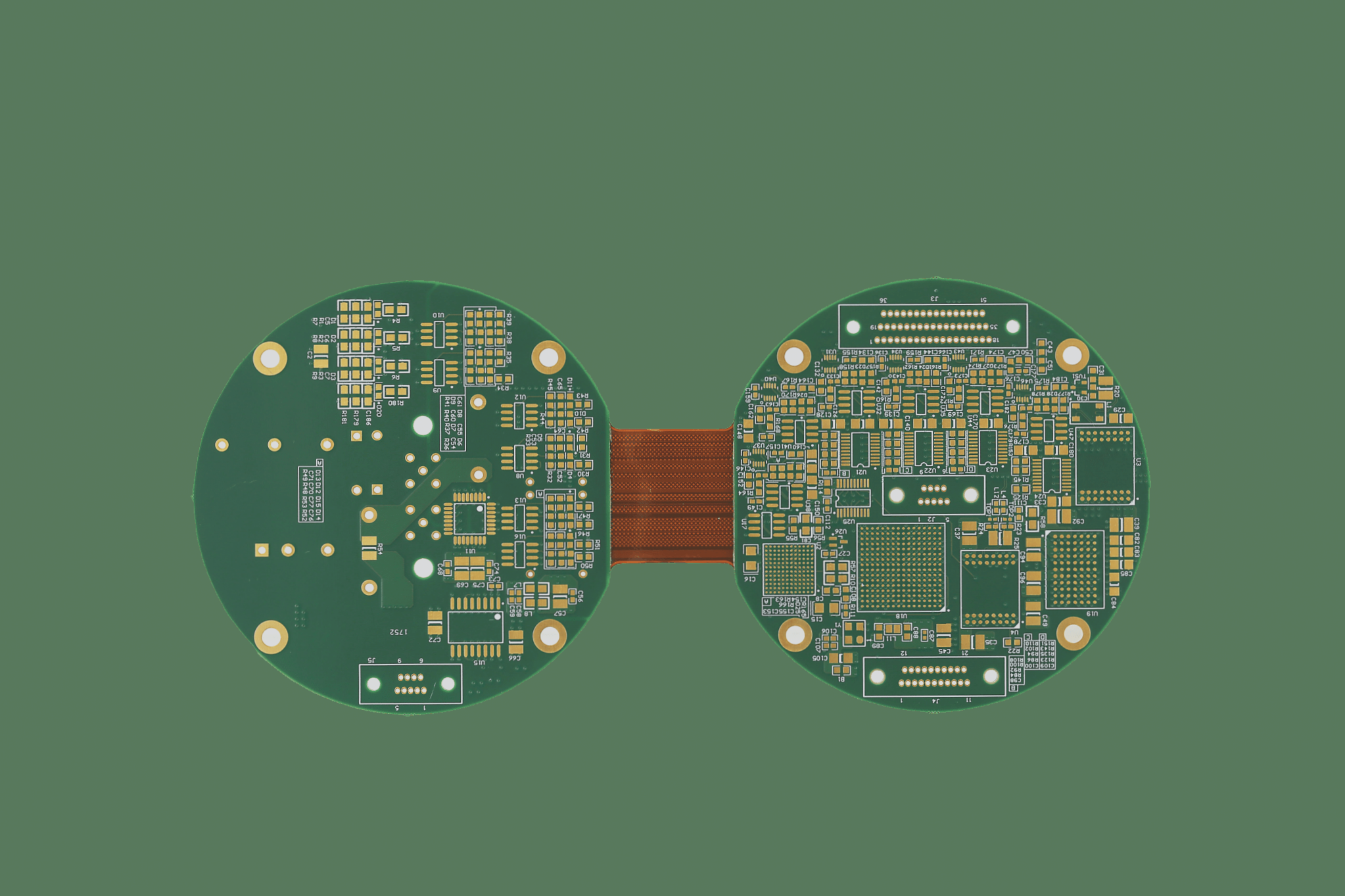
Industrial requirements are evolving, with a growing emphasis on heavy copper PCB designs. These specialized PCBs are becoming increasingly vital in the electronics industry, particularly for intricate switches that need to fit into tight spaces. The exceptional electrical and thermal conductivity of copper makes it a preferred choice for such applications.
Key Features of Heavy Copper PCBs:
- Multi-layered or double-sided boards
- Detailed exterior layers
- Heavy copper layers in the interior
Heavy copper PCBs are commonly found in power converters and planar transformers due to their unique design and capabilities.
Advantages of Heavy Copper PCBs:
- Versatility: These boards are adaptable across various devices with different power and signal levels.
- Compact Size: They can handle high frequencies, currents, temperatures, and thermal cycles, reducing overall board size and weight.
- Thermal Resistance: Enhanced conductivity allows for better heat dissipation and improved thermal stress resistance.
- Improved Current Handling: Copper vias reduce current-sharing issues associated with parallel traces.
- Structural Integrity: Multi-layered construction offers increased mechanical strength.
Manufacturing Techniques:
Specialized plating and etching processes are employed to increase copper thickness on sidewalls and plated holes, ensuring even distribution across the PCB.
Notable Fabrication Methods:
- Blue Bar Method: Efficiently handles higher currents and reduces manufacturing costs.
- Embedded Copper Method: Incorporates thick copper into the prepreg resin, with copper thickness determined by resin thickness.
Distinguishing Factors:
Heavy copper PCBs stand out from standard PCBs due to their thicker copper layers, ranging from 4 oz to 20 oz, enabling them to conduct significantly higher currents and excel in heat dissipation and mechanical robustness.
While heavy copper PCBs may be costlier to produce, their benefits in demanding applications where high energy and reliability are crucial often justify the investment.
When selecting manufacturers for heavy copper PCBs, prioritize those capable of meeting specific requirements and delivering consistent performance and thermal management capabilities.


